Working of NPN and PNP transistor - Electronics, Physics - eSaral
Table of Contents

Hey, do you want to learn about the Working of NPN and PNP transistor? if yes. Then you are at the right place.
The holes of the P region (emitter) are rippled by the positive terminal of battery $\mathrm{V}_{\mathrm{EE}}$ towards the base. The potential barrier at the emitter junction is reduced as it is forward bias and hence the holes cross this junction and penetrate into the N region. This constitutes the emitter current. The width of the base region is very thin and it is lightly doped and hence only two to five percent of the holes recombine with the free electrons of the N region. This constitutes the base current $\mathrm{I}_{\mathrm{B}}$. which of course, is very small. The remaining holes (95% to 98%) are able to drift across the base and enter into the collector region. This constitutes the collector current.
Working:
The electron in the emitter region is rippled from the negative terminal of the battery towards the emitter junction. Since the potential barrier at the junction is reduced due to forward bias and the base region is very thin and lightly doped, electrons cross the p-type base region. A few electrons combine with the holes in P-region and are lost as the charge carriers. Now the electrons in N-region (collector region) readily swept up by the positive collector voltage $\mathrm{V}_{\mathrm{CC}}$.
The current conduction in the N-P-N transistor is carried out by electrons.
Common base (CB)
Common emitter (CE)
Common collector (CC)
The term ‘Common’ is used to denote the transistor lead which is common to the input and the output.
In this configuration the input signal is applied between emitter and base and the output is taken from collector and base.
In common base as an amplifier phase difference between input and output is zero.
In common emitter as an amplifier phase difference between input and output is $\pi$.
In this case, $\mathrm{I}_{\mathrm{B}}$ increases less rapidly with $V_{B E}$ as compared to common-base configuration. This shows input resistance of the common-emitter circuit is higher than that of the common-base circuit.
Relationship between $\alpha, \beta$ and $\gamma$:
Emitter current $I_{E}=I_{B}+I_{C}$......(1)
divide by $\mathrm{I}_{\mathrm{C}}$ gives, $\frac{\mathrm{I}_{\mathrm{E}}}{\mathrm{I}_{\mathrm{C}}}=\frac{\mathrm{I}_{\mathrm{B}}}{\mathrm{I}_{\mathrm{C}}}+1$
or
$\frac{1}{\alpha}=\frac{1}{\beta}+1$
$\beta=\frac{\alpha}{1-\alpha}$
So, that's all from this blog, I hope you get the idea about the Working of NPN and PNP transistor. If you enjoyed this explanation then don't forget to share it with your friends.
Also, read
What is Transistor
To watch Free Learning Videos on physics by Saransh Gupta sir Install the eSaral App.
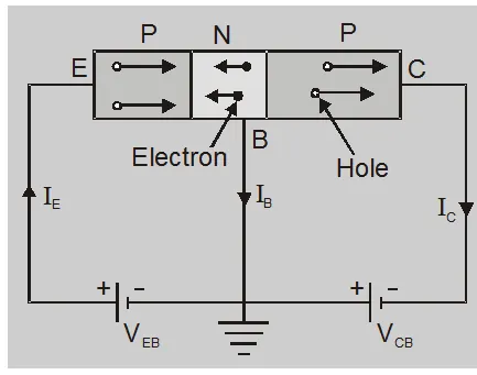
P-N-P Transistor:
The holes of the P region (emitter) are rippled by the positive terminal of battery $\mathrm{V}_{\mathrm{EE}}$ towards the base. The potential barrier at the emitter junction is reduced as it is forward bias and hence the holes cross this junction and penetrate into the N region. This constitutes the emitter current. The width of the base region is very thin and it is lightly doped and hence only two to five percent of the holes recombine with the free electrons of the N region. This constitutes the base current $\mathrm{I}_{\mathrm{B}}$. which of course, is very small. The remaining holes (95% to 98%) are able to drift across the base and enter into the collector region. This constitutes the collector current.
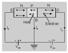
N-P-N Transistor:
Working:
The electron in the emitter region is rippled from the negative terminal of the battery towards the emitter junction. Since the potential barrier at the junction is reduced due to forward bias and the base region is very thin and lightly doped, electrons cross the p-type base region. A few electrons combine with the holes in P-region and are lost as the charge carriers. Now the electrons in N-region (collector region) readily swept up by the positive collector voltage $\mathrm{V}_{\mathrm{CC}}$.
The current conduction in the N-P-N transistor is carried out by electrons.
Transistor configuration
Three types of transistor circuit configuration areCommon base (CB)
Common emitter (CE)
Common collector (CC)
The term ‘Common’ is used to denote the transistor lead which is common to the input and the output.
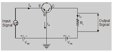
Common Base Configuration
In this configuration the input signal is applied between emitter and base and the output is taken from collector and base.
In common base as an amplifier phase difference between input and output is zero.
Characteristics:
Input characteristic:
The curve between emitter current $\mathrm{I}_{\mathrm{E}}$ and emitter base voltage $V_{\mathrm{EB}}$ at constant collector base voltage $\mathrm{V}_{\mathrm{CB}}$ represents the input characteristics. Collector base voltage $\mathrm{V}_{\mathrm{CB}}$ is kept fixed.- There exist a cut in, offset or threshold voltage $V_{\mathrm{EB}}$ below which the emitter current is very small.
- The emitter current $\mathrm{I}_{\mathrm{E}}$ increases rapidly with small increase in emitter-base voltage $V_{\mathrm{EB}}$. This shows that the input resistance is very small.
Output characteristic:
Curve between collector current $\mathrm{I}_{\mathrm{C}}$ and collector base voltage $V_{\mathrm{CB}}$ at constant emitter $\mathrm{I}_{\mathrm{E}}$ represents the output characteristic.Common emitter configuration
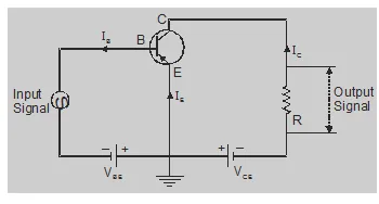
In this configuration the input signal is applied between base and emitter and the output is taken from collector and emitter.
In common emitter as an amplifier phase difference between input and output is $\pi$.
Characteristic
Input characteristics:
The curve between base current $\mathrm{I}_{\mathrm{B}}$ and base emitter voltage $\mathrm{V}_{\mathrm{BE}}$ at constant collector-emitter voltage $\mathrm{V}_{\mathrm{CE}}$ represents the input characteristic.In this case, $\mathrm{I}_{\mathrm{B}}$ increases less rapidly with $V_{B E}$ as compared to common-base configuration. This shows input resistance of the common-emitter circuit is higher than that of the common-base circuit.
Output characteristic:
The curve between collector current $\mathrm{I}_{\mathrm{C}}$ and collector emitter voltage $V_{C E}$ at constant base current $\mathrm{I}_{\mathrm{B}}$ represents the output characteristic.Relationship between $\alpha, \beta$ and $\gamma$:
Emitter current $I_{E}=I_{B}+I_{C}$......(1)
divide by $\mathrm{I}_{\mathrm{C}}$ gives, $\frac{\mathrm{I}_{\mathrm{E}}}{\mathrm{I}_{\mathrm{C}}}=\frac{\mathrm{I}_{\mathrm{B}}}{\mathrm{I}_{\mathrm{C}}}+1$
or
$\frac{1}{\alpha}=\frac{1}{\beta}+1$
$\beta=\frac{\alpha}{1-\alpha}$
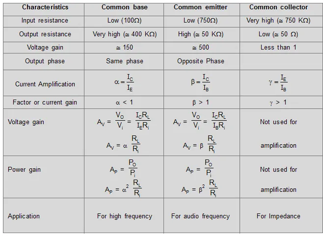
Comparison table between CB, CE and CC configuration
So, that's all from this blog, I hope you get the idea about the Working of NPN and PNP transistor. If you enjoyed this explanation then don't forget to share it with your friends.
Also, read
What is Transistor
To watch Free Learning Videos on physics by Saransh Gupta sir Install the eSaral App.