NCERT Solutions for Class 12 Physics Chapter 14 Semiconductor Electronics PDF - eSaral

NCERT Solutions for Class 12 Physics Chapter 14 Semiconductor Electronics PDF
Hey, are you a class 12 student and looking for ways to download NCERT Solutions for Class 12 Physics Chapter 14 Semiconductor Electronics PDF? If yes. Then read this post till the end.In this article, we have listed NCERT Solutions for Class 12 Physics Chapter 14 Semiconductor Electronics in PDF that are prepared by Kota’s top IITian Faculties by keeping Simplicity in mind.
If you want to learn and understand class 12 Physics Chapter 14 "Semiconductor Electronics" in an easy way then you can use these solutions PDF.
NCERT Solutions helps students to Practice important concepts of subjects easily. Class 12 Physics solutions provide detailed explanations of all the NCERT questions that students can use to clear their doubts instantly.
If you want to score high in your class 12 Physics Exam then it is very important for you to have a good knowledge of all the important topics, so to learn and practice those topics you can use eSaral NCERT Solutions.
In this article, we have listed NCERT Solutions for Class 12 Physics Chapter 14 Semiconductor Electronics PDF that you can download to start your preparations anytime.
So, without wasting more time Let’s start.
Download NCERT Solutions for Class 12 Physics Chapter 14 Semiconductor Electronics PDF
Question 1. In an $n$-type silicon, which of the following statement is true:
(a) Electrons are majority carriers and trivalent atoms are the dopants.
(b) Electrons are minority carriers and pentavalent atoms are the dopants.
(c) Holes are minority carriers and pentavalent atoms are the dopants.
(d) Holes are majority carriers and trivalent atoms are the dopants.
Solution: (c) In an n-type of semiconductors, the electrons are the majority carrier, holes are minority carrier. The n-type semiconductor is obtained when pentavalent atoms are doped into silicon.
vQuestion 2. Which of the statements given in Exercise 14.1 is true for p-type semiconductors?
Solution. The statement is (d) true.
It is because in a p-type semiconductor, the holes are the majority carriers and the electrons are the minority carriers. The p-type semiconductor is obtained when a trivalent atom is doped into silicon.
is obtained when a trivalent atom is doped into silicon.
Question 3. Carbon, silicon and germanium have four valence electrons each. These are characterised by valence and conduction bands separated by energy band gap respectively equal to $(\mathrm{Eg})_{\mathrm{C}},(\mathrm{Eg})_{\mathrm{Si}}$ and $(\mathrm{Eg})_{\mathrm{Ge}} .$ Which of the following statements is true?
(a)$(\mathrm{Eg})_{\mathrm{Si}}<(\mathrm{Eg})_{\mathrm{Ge}}<(\mathrm{Eg})_{\mathrm{C}}$
(b)$(\mathrm{Eg})_{\mathrm{C}}<(\mathrm{Eg})_{\mathrm{Ge}}>(\mathrm{Eg})_{\mathrm{Si}}$
(c)$(\mathrm{Eg})_{\mathrm{C}}>(\mathrm{Eg})_{\mathrm{Si}}>(\mathrm{Eg})_{\mathrm{Ge}}$
(d)$\quad(\mathrm{Eg})_{\mathrm{C}}=(\mathrm{Eg})_{\mathrm{Si}}=(\mathrm{Eg})_{\mathrm{Ge}}$
Solution: (c)
The energy band gap is maximum for carbon, for silicon and least for germanium out of the given three elements.
Question 4. In an unbiased $\mathrm{p}-\mathrm{n}$ junction, holes diffuse from the p-region to n-region because
(a) free electrons in the n-region attract them.
(b) they move across the junction by the potential difference.
(c) hole concentration in p-region is more as compared to n-region.
(d) All the above.
Solution: (c)
In unbiased p-n junction, holes diffuse from the p-region to n-region because hole concentration in p-region is more compared to n-junction. As the diffusion of charge carriers across the junction takes place from higher concentration to lower concentration.
Question 5. When a forward bias is applied to a p-n junction, it
(a) raises the potential barrier.
(b) reduces the majority carrier current to zero.
(c) lowers the potential barrier.
(d) none of the above.
Solution: (c)
When we apply a forward bias on a p-n junction then the value of the potential barrier is lowered. Also, the potential barrier opposes the applied voltage. This reduces the potential barrier across the junction.
Question 6. For transistor action, which of the following statements are correct:
(a) Base, emitter and collector regions should have similar size and doping concentrations.
(b) The base region must be very thin and lightly doped.
(c) The emitter junction is forward biased and collector junction is reverse biased.
(d) Both the emitter junction as well as the collector junction are forward biased.
Solution: (b), (c).
For a transistor, its junction is lightly doped and the base region is very thin. Also, the emitter junction of a transistor must be forward-biased and collector junction should be reverse-biased.
Question 7. For a transistor amplifier, the voltage gain
(a) remains constant for all frequencies.
(b) is high at high and low frequencies and constant in the middle frequency range.
(c) is low at high and low frequencies and constant at mid frequencies.
(d) none of the above.
Solution: (c)
For a transistor amplifier, the voltage gain is low at high and low frequencies and constant at mid frequencies. It is constant at mid-frequency range only.
Question 8. In half-wave rectification, what is the output frequency if the input frequency is $50 \mathrm{~Hz}$. What is the output frequency of a full-wave rectifier for the same input frequency?
Solutiion. Given:
Input frequency $=50 \mathrm{~Hz}$
We know that for a half-wave rectifier, the output frequency is equal to the input frequency.
$\therefore$ Output frequency $=50 \mathrm{~Hz}$
And for a full-wave rectifier, the output frequency is twice the input frequency.
$\therefore$ Output frequency $=2 \times 50=100 \mathrm{~Hz}$
Question 9. For a CE-transistor amplifier, the audio signal voltage across the collected resistance of $2 \mathrm{k} \Omega$ is $2 \mathrm{~V}$. Suppose the current amplification factor of the transistor is 100 , find the input signal voltage and base current if the base resistance is $1 \mathrm{k} \Omega$.
Solution: Given:
Collector resistance, $R_{C}=2 k \Omega=2000 \Omega$
Audio signal voltage across the collector resistance, $V=2 \mathrm{~V}$
Current amplification factor of the transistor. $\beta=100$
Base resistance, $R_{B}=1 \mathrm{k} \Omega=1000 \Omega$
Input signal voltage $=V_{i}$
Base current $=I_{B}$
We have the amplification relation as: $\frac{V}{V_{i}}=\beta \frac{R_{c}}{R_{b}}$ Voltage amplification, $V_{i}=V \frac{R_{b}}{\beta R_{c}}=\frac{2 \times 1000}{100 \times 2000}=0.01 \mathrm{~V}$
Base resistance, $R_{B}=\frac{V_{i}}{I_{B}}=\frac{0.01}{1000}=10 \mu \mathrm{A}$
Question 10. Two amplifiers are connected one after the other in series (cascaded). The first amplifier has a voltage gain of 10 and the second has a voltage gain of 20 . If the input signal is $0.01$ volt, calculate the output ac signal.
Solution. Given:
The voltage gain of the first amplifier, $V_{1}=10$
The voltage gain of the second amplifier, $V_{2}=20$
The voltage of the input signal, $V_{i}=0.01 \mathrm{~V}$
The voltage of output $\mathrm{AC}$ signal $=V_{o}$
The total voltage gain of a two-stage amplifier is given by the product of voltage gains of both the stages,
i.e., $V=V_{1} \times V_{2}=10 \times 20=200$
It can be calculated by the relation: $V=\mathrm{Vo} / \mathrm{Vi}$
$V_{0}=V \times V_{i}=200 \times 0.01=2 \mathrm{~V}$
Question 11. A p-n photodiode is fabricated from a semiconductor with band gap of $2.8 \mathrm{eV}$. Can it detect a wavelength of $6000 \mathrm{~nm}$ ?
Solution. Given:
The energy band gap of the given photodiode, $E_{g}=2.8 \mathrm{eV}$
The wavelength, $\lambda=6000 \mathrm{~nm}=6000 \times 10^{-9} \mathrm{~m}$
The energy of a photon is given by the relation $E=h c / \lambda$
Where, $\mathrm{h}=$ Planck's constant $=6.626 \times 10^{-34} \mathrm{~J} \mathrm{~s}$
$\mathrm{c}=$ Speed of light $=3 \times 10^{8} \mathrm{~m} / \mathrm{s}$
$E=\frac{6.626 \times 10^{-34} \times 3 \times 10^{8}}{6000 \times 10^{-9}}=3.313 \times 10^{-20} \mathrm{~J}$
But $1.6 \times 10^{-19} \mathrm{~J}=1 \mathrm{eV}$
$E=3.313 \times 10^{-20} \mathrm{~J}$
$\therefore \mathrm{E}=3.313 \times 10^{-20} \mathrm{~J}=3.313 \times 10^{-20} / 1.6 \times 10^{-19}=0.207 \mathrm{eV}$
The energy of wavelength $6000 \mathrm{~nm}$ is $0.207 \mathrm{eV}$, which is less than $2.8 \mathrm{eV}$ (the energy band gap of a photodiode). Hence, the photodiode cannot detect the signal.
Question 12. The number of silicon atoms per $m^{3}$ is $5 \times 10^{28}$. This is doped simultaneously with $5 \times 10^{22}$ atoms per $\mathrm{m}^{3}$ of Arsenic and $5 \times 10^{20}$ per $\mathrm{m}^{3}$ atoms of Indium. Calculate the number of electrons and holes. Given that $n_{i}=1.5 \times 10^{16} \mathrm{~m}^{-3}$. Is the material $\mathrm{n}$-type or $\mathrm{p}$-type?
Solution. Number of silicon atoms, $\mathrm{N}=5 \times 10^{28}$ atoms $/ \mathrm{m}^{3}$
Number of arsenic atoms, $n_{A s}=5 \times 10^{22}$ atoms $/ \mathrm{m}^{3}$
Number of indium atoms, $n_{I n}=5 \times 10^{20}$ atoms $/ \mathrm{m}^{3}$
Number of thermally generated electrons, $n_{i}=1.5 \times 10^{16}$ electrons $/ \mathrm{m}^{3}$
Number of electrons, $n_{e}=5 \times 10^{22}-1.5 \times 10^{16} \approx 4.99 \times 10^{22}$
Number of holes $=n_{h}$
In thermal equilibrium, the concentrations of electrons and holes in a semiconductor are related as: $n_{e} n_{h}=n_{i}^{2}$
Therefore, $n_{h}=\frac{n_{i}^{2}}{n_{e}}=\frac{\left(1.5 \times 10^{16}\right)^{2}}{4.99 \times 10^{22}} \approx 4.51 \times 10^{9}$
Therefore, the number of electrons is approximately $4.99 \times 10^{22}$ and the number of holes is about $4.51 \times 10^{9}$. Since the number of electrons is more than the number of holes, the material is an $\mathrm{n}$-type semiconductor.
Question 13. In an intrinsic semiconductor the energy gap $E_{g}$ is $1.2 \mathrm{eV}$. Its hole mobility is much smaller than electron mobility and independent of temperature. What is the ratio between conductivity at $600 \mathrm{~K}$ and that at $300 \mathrm{~K}$ ? Assume that the temperature dependence of intrinsic carrier concentration $n_{i}$ is given by $n_{i}=$ $n_{0} \exp \left(-\frac{E_{g}}{2 k_{B} T}\right)$ where $n_{0}$ is a constant.
Solution. Given
Energy gap $\left(E_{g}\right)=1.2 \mathrm{eV}$
The temperature dependence of intrinsic carrier concentration $n_{i}$ is given by
$n_{i}=n_{0} \exp \left(-\frac{E_{g}}{2 k_{B} T}\right)$
At temperature $T_{1}=600 \mathrm{~K}$
$n_{1}=n_{0} \exp \left(-\frac{E_{g}}{2 k_{B} \times 600}\right)$ $\cdots$(1)
At temperature $T_{1}=300 \mathrm{~K}$
$n_{2}=n_{0} \exp \left(-\frac{E_{g}}{2 k_{B} \times 300}\right)$ $\cdots$(2)
By dividing equation (1) and (2)
$\frac{n_{1}}{n_{2}}=\frac{n_{0} \exp \left(-\frac{E_{g}}{2 k_{B} \times 600}\right)}{n_{0} \exp \left(-\frac{E_{g}}{2 k_{B} \times 300}\right)}$
$\Rightarrow \frac{n_{1}}{n_{2}}=\exp \left(-\frac{E_{g}}{2 k_{B}}\left(\frac{1}{600}-\frac{1}{300}\right)\right)$
$\Rightarrow \frac{n_{1}}{n_{2}}=\exp \left(\frac{E_{g}}{2 k_{B}}\left(\frac{1}{600}\right)\right)=\exp \left(\frac{1.2 \mathrm{eV}}{2 \times 8.62 \times 10^{-5} \mathrm{eV} \mathrm{K}^{-1} \times 600 \mathrm{~K}}\right)$
$\Rightarrow \frac{n_{1}}{n_{2}}=\exp (11.6)$
$\Rightarrow \frac{n_{1}}{n_{2}}=1.091 \times 10^{5}$
Hence, the ratio of conductivity at $600 \mathrm{~K}$ and $300 \mathrm{~K}$ is $1.091 \times 10^{5}$.
Question 14. In a p-n junction diode, the current I can be expressed as
$I=I_{0} \exp \left(\frac{e V}{k_{B} T}-1\right)$
where $I_{0}$ is called the reverse saturation current, $V$ is the voltage across the diode and is positive for forward bias and negative for reverse bias, and $\mathrm{I}$ is the current through the diode, $\mathrm{kB}$ is the Boltzmann constant $\left(8.6 \times 10^{-5} \mathrm{eV} / \mathrm{K}\right)$ and $\mathrm{T}$ is the absolute temperature. If for a given diode $I_{0}=5 \times 10^{-12} \mathrm{~A}$ and $T=$ $300 \mathrm{~K}$, then
(a) What will be the forward current at a forward voltage of $0.6 \mathrm{~V}$ ?
(b) What will be the increase in the current if the voltage across the diode is increased to $0.7 \mathrm{~V} ?$
(c) What is the dynamic resistance?
(d) What will be the current if reverse bias voltage changes from $1 \mathrm{~V}$ to 2 V?
Solution: Given: The current $I$ in a p-n junction diode, $I=I_{0} \exp \left(\frac{e V}{k_{B} T}-1\right)$
$I_{0}=5 \times 10^{-12} \mathrm{~A}$
$T=300 \mathrm{~K}$
$K_{B}=8.6 \times 10^{-5} \mathrm{eV} / \mathrm{K}$
(a) Forward voltage $0.6 \mathrm{~V}$
$I=5 \times 10^{-12} \exp \left(\frac{0.6}{8.6 \times 10^{-5} \times 300}-1\right)$
$\Rightarrow I=5 \times 10^{-12} \exp (22.25)=0.0231 \mathrm{~A}$
The forward current in the diode is $0.0231 \mathrm{~A}$.
(b) Forward voltage $0.7 \mathrm{~V}$
$I=5 \times 10^{-12} \exp \left(\frac{0.7}{8.6 \times 10^{-5} \times 300}-1\right)$
$\Rightarrow I=5 \times 10^{-12} \exp (26.13)=1.116 \mathrm{~A}$
The forward current in the diode is $1.116 \mathrm{~A}$.
(c) Dynamic Resistance is given as the ratio of change in voltage and change in current.
Dynamic Resistance $=\frac{\text { change in voltage }}{\text { change in current }}=\frac{0.7-0.6}{1.116-0.0231}=\frac{0.1}{1.093}=$
$0.091 \Omega$
(d) If we change the reverse bias voltage from $1 \mathrm{~V}$ to $2 \mathrm{~V}$, then the current will remain the same as $I_{0}$ in both cases. Hence, the dynamic resistance in reverse bias will be infinite.
Question 15. You are given the two circuits as shown in Fig. $14.44$. Show that circuit (a) acts as OR gate while the circuit (b) acts as AND gate.
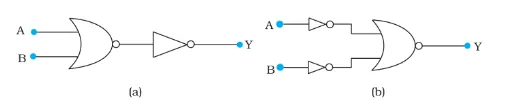
FIGURE $14.44$
Solution: (a) The left half of the circuit is NOR gate and the right half is NOT.
Hence the output from the NOR gate will be $\overline{A+B}$
Again the output of this signal through NOT gate will be,
$\overline{\overline{A+B}}=A+B$
$\therefore Y=A+B$
Hence the circuit is an OR gate.
(b) The output of this logic gate is NOR gate over the output of two NOT gate.
$\therefore Y=\overline{\bar{A}+\bar{B}}=\overline{\bar{A}} \cdot \overline{\bar{B}}=A \cdot B$
Hence the circuit is an AND gate.
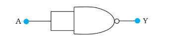
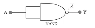
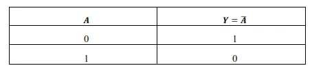
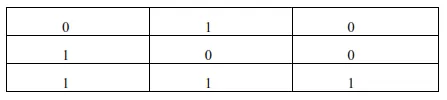
Question 16. Write the truth table for a NAND gate connected as given in Fig. $14.45$.
Hence identify the exact logic operation carried out by this circuit.
Solution:
A is the two input for the NAND gate. Hence its output will be
$Y=\overline{A \cdot A}=\bar{A}+\bar{A}=\bar{A}$
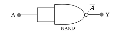
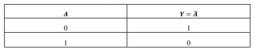
The truth table can be drawn as
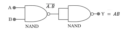
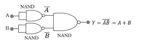
Question 17. You are given two circuits as shown in Fig. $14.46$, which consist of NAND gates. Identify the logic operation carried out by the two circuits.
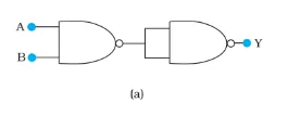
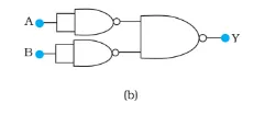
FIGURE $14.46$
Solution: (a) The output from the $1^{\text {st }}$ NAND gate will be $\overline{A \cdot B}$. Now the output from the second NAND gate will be $\overline{(\overline{A . B}) \cdot(\overline{A . B})}$
$\therefore Y=\overline{(\overline{A \cdot B})}+\overline{(\overline{A \cdot B})}=A B+A B=A B$
(b) For the $1^{\text {st }}$ two NAND gate, the output will be
$Y_{1}=\overline{A \cdot A}=\bar{A}+\bar{A}=\bar{A}$
And $Y_{2}=\overline{B \cdot B}=\bar{B}+\bar{B}=\bar{B}$
The final output will be
$Y=\overline{\bar{A} \bar{B}}=\overline{\bar{A}}+\overline{\bar{B}}=A+B$
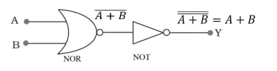
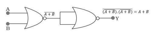
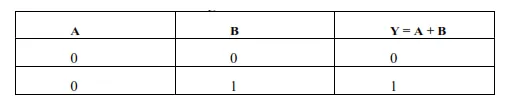
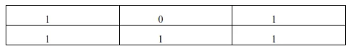
Question 18. Write the truth table for circuit given in Fig. $14.47$ below consisting of NOR gates and identify the logic operation (OR, AND, NOT) which this circuit is performing.
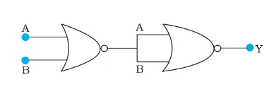
FIGURE 14.47
(Hint: $\mathrm{A}=0, \mathrm{~B}=1$ then $\mathrm{A}$ and $\mathrm{B}$ inputs of second NOR gate will be 0 and hence $\mathrm{Y}=1$. Similarly work out the values of $\mathrm{Y}$ for other combinations of $\mathrm{A}$ and $\mathrm{B}$. Compare with the truth table of OR, AND, NOT gates and find the correct one.)
Solution. A and B are input for NOR gate, and the output will be $\overline{A+B}$.
The output from the second NOR gate will be $\overline{(\overline{A+B}) \cdot(\overline{A+B})}=\overline{\overline{A+B}}+$
$\overline{\overline{A+B}}=A+B$
The truth table of the following circuit is
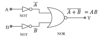
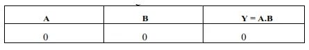
Question 19. Write the truth table for the circuits given in Fig. $14.48$ consisting of NOR gates only. Identify the logic operations (OR, AND, NOT) performed by the two circuits.
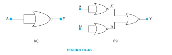 Solution: (a) A is the two input for the NAND gate. Hence its output will be
$Y=\overline{A \cdot A}=\bar{A}+\bar{A}=\bar{A}$
The truth table can be drawn as
(b) $\bar{A}$ and $\bar{B}$ are the input for the last NOR gate. Hence, the output will be
$Y=\overline{\bar{A}+\bar{B}}=\overline{\bar{A}} \cdot \overline{\bar{B}}=A \cdot B$
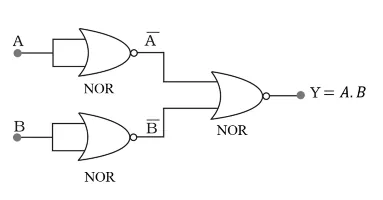
The truth table of the following circuit is
Also Read,
Class 12 Physics Notes Download.
Class 12 Physics Book Chapterwise Download.
Class 11 Physics Exemplar Chapterwise Download.
If you have any Confusion related to NCERT Solutions for Class 12 Physics Chapter 14 Semiconductor Electronics PDF then feel free to ask in the comments section down below.
To watch Free Learning Videos on Class 12 Physics by Kota’s top IITan’s Faculties Install the eSaral App