Semiconductor Class 12 Important Questions — Fully Solved (CBSE Boards & JEE Main)

Table of Contents


eSaral › Class 12 › Physics › Semiconductor Class 12 Important Questions
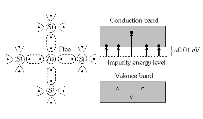
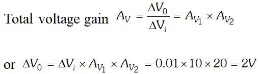
Get important questions of Semiconductor Class 12 for Boards exams. View the Physics question bank for Class 11 & 12. These important questions will play significant role in clearing concepts of Semiconductor chapter. This question bank is designed keeping NCERT in mind and the questions are updated with respect to upcoming Board exams. You will get here all the important questions for class 12 Physics chapters. Click Here for Detailed Chapter-wise Notes of PHYSICS for Class 12th, JEE & NEET. Draw the voltage current characteristic of a zener diode 1. Biasing determines behaviour: The direction of bias (forward or reverse) fundamentally changes how a p-n junction behaves — from a conductor (forward) to a near-insulator (reverse). All diode applications flow from this principle. 2. Zener diodes exploit breakdown: Unlike regular diodes that must avoid breakdown, zener diodes are designed to operate there — the flat V-I curve in the breakdown region is what makes voltage regulation possible. 3. Transistor sensitivity = exam opportunity: Temperature sensitivity and the transistor oscillator are high-probability 3–5 mark questions in Board exams. Practice the circuit diagrams and step-by-step working explanations for both. For concept-level clarity before your Board exam or JEE Main preparation, the IIT Bombay faculty at eSaral — including Kota-trained teachers with verified All India Ranks — have created detailed video lectures and practice test series for every topic in this chapter. Students from eSaral's 2023 batch secured top percentile scores in JEE Main Physics using the same structured approach reflected in this question bank. Explore more resources: Find answers to common questions. A half-wave rectifier uses one diode and converts only the positive half-cycle of AC into DC — output frequency equals input frequency (50 Hz). A full-wave rectifier uses two diodes (or four in a bridge circuit) and converts both half-cycles — output frequency is double the input (100 Hz). Full-wave rectifiers are more efficient and produce smoother DC output. As per the latest CBSE Class 12 Physics syllabus (Unit IX: Electronic Devices), the Semiconductor chapter carries approximately 7 marks in the theory examination. This includes 2-mark short answer questions, 3-mark questions requiring diagrams (such as rectifier circuits), and occasionally 5-mark questions on transistor working or zener diode voltage regulation. The most important topics are: p-n junction diode (forward/reverse bias, V-I characteristics), zener diode as voltage stabilizer, half-wave and full-wave rectifiers, transistor characteristics and action (CE configuration), LED and photodiode working, and the difference between intrinsic and extrinsic semiconductors. These topics together account for 7–8 marks in most CBSE Board papers. Doping adds either pentavalent (donor) or trivalent (acceptor) impurity atoms to a pure semiconductor. This creates additional free electrons (N-type) or holes (P-type), significantly increasing the number of charge carriers available for conduction. Even a doping level of 1 impurity atom per 10 million semiconductor atoms can increase electrical conductivity by several orders of magnitude compared to the intrinsic semiconductor. The output frequency of a full-wave rectifier is 100 Hz when the input AC frequency is 50 Hz. This is because both the positive and negative half-cycles of the input are converted into unidirectional pulses, effectively doubling the number of output pulses per second compared to the input A zener diode works as a voltage regulator because in the reverse breakdown region, the voltage across it (zener voltage, V_Z) remains nearly constant even when the current through it changes significantly. Any fluctuation in the input voltage is absorbed by the series resistor R, while the load connected across the zener always receives a stable, regulated output voltage equal to V_Z.India's Best Exam Preparation for Class 12th - Download Now
India's Best Exam Preparation for Class 12th - Download Now
 (ii) P-type semiconductor : When a pure semiconductor say silicon (having four valence electron) doped with a trivalent impurity say Aluminium (having three valence electron) the impurity atom will replace the Si atom as shown in figure. The three valence electrons of impurity atom will form covalent bonds by sharing the electrons of the adjoining atoms of Si while there will be one incomplete covalent bond with a neighbouring Si atom due to the deficiency of an electron. This deficiency is completed by taking an electron from one of the Si-Si bonds. This makes Al ionised (negatively charged) and creates hole. This type of semi conductor is called P-type semiconductor. In P-type semiconductor, impurity is called acceptor impurity and the net charge of the crystal as a whole is zero. Holes are majority charge carriers and electrons are minority charge carriers in such type of semiconductors.
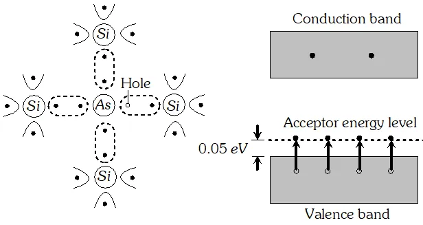
![]() As a voltage stabilizer
As a voltage stabilizer 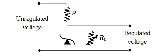 The unregulated dc voltage (filtered output of a rectifier) is connected to the zener diode through a series resistance R such that the zener diode is reverse biased. If the input voltage increases, the current through R and zener diode also increases. This increases the voltage drop across R without any change in the voltage across the zener diode. This is because in the breakdown region, zener voltage remains constant even through the current through the zener diode changes. Thus any increase or decrease in input voltage results in increase or decrease of the voltage drop across R without any change in voltage across the zener diode. Thus the zener diode acts as a voltage regulator.
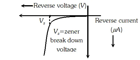
 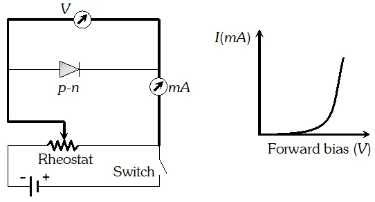 Figure below show a reverse biased p-n junction and its voltage current graph
 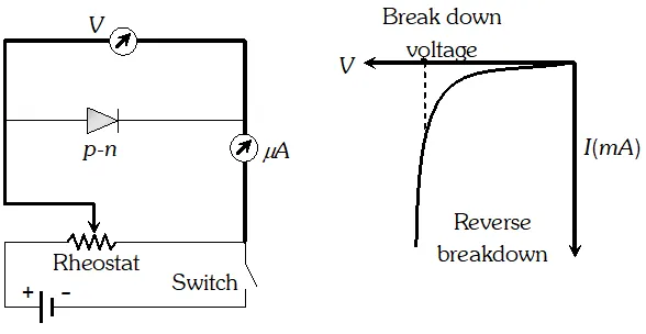 In both cases, the battery is connected to the p-n junction through a rheostat so that the applied voltage can be changed. For different values of voltages, the value of current in noted. A graph is plotted between V and I.
 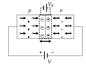 Reverse Biasing : A P-N junction is said to be reverse biased if the positive terminal of the external battery is connected to n-side and the negative terminal to p-side. In reverse biased the height of barrier potential and width of depletion region increases. The resistance of p-n junction is high to the flow of current when reverse biased.
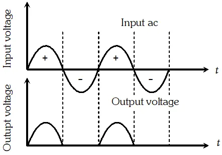
  A half-wave rectifier consists of a single diode, as shown in the circuit diagram. The secondary of the transformer gives the desired ac voltage across A and B. When the voltage at A is positive, the diode is forward biased and it conducts current. When A is negative, the diode is reverse biased and it does into conduct current. Thus we get output across RL during positive half-cycles only. The output is unidirectional but varying.
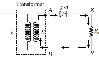
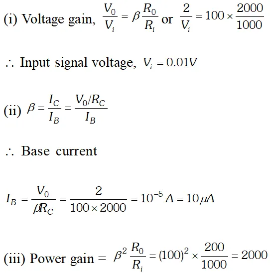
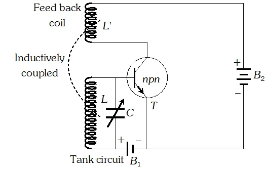 $L, L^{\prime} \rightarrow$ Inductive coils, $C \rightarrow$Variable capacitor, $T \rightarrow$ Transistor (NPN), ® Low tension battery for forward biasing of emitter base junction of transistor, A high tension battery for reverse biasing of collector emitter junction of transistor. Tank circuit ® consists of L and C in parallel, it can produce electrical oscillations of frequency $v=\frac{1}{2 \pi \sqrt{L C}}$ Working : The coil L’ is inductively coupled with the coil L of the tank circuit in such away that if increasing magnetic flux is linked with L it supports the forward bias of base emitter circuit and if decreasing magnetic flux is linked with L, it opposes the forward bias of the base emitter circuit. When the key K is closed, a small collector current starts growing due to L’. As a result, an increasing magnetic flux is linked with L’ and hence with L. Due to this increasing magnetic flux, an emf is induced in L which supports the forward biasing of the base-emitter circuit so emitter current increases which in turn increases the collector current. The increase in collector current increases the magnetic flux linked with L’ and hence with L. Therefore more emf is induced in L which further support the forward biasing of base emitter circuit. The emitter current and hence the collector current further increases. The process continues till the collector current reaches saturation and capacitor gets fully charged. As the current through L’ stops changing, the emf induced in L vanishes. As a result, the support to the forward biasing of the base-emitter circuit is with drawn and the capacitor C is discharged through L. Due to the vanishing of induced emf, the emitter current and hence the collector current decreases. Therefore a decreasing magnetic flux is linked with L’ and hence with L. This induced emf in L which opposes the forward biasing of the base-emitter circuit. This result in further decrease in emitter current and hence in collector current. This process continue till the collector current becomes zero. The induced emf in L again becomes zero and the opposition to the forward biasing of the base emitter circuit is with drawn. The capacitor is discharged through L. The emitter current and hence the collector current again starts increasing. The cycle repeats again and again.
 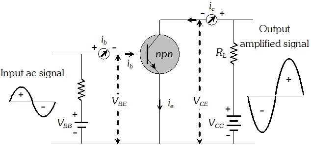 $V_{B B}=$ Low tension battery for forward biasing base- emitter circuit $V_{C C}=$ High tension battery for reverse biasing collector-emitter circuit $V_{B E}=$ Potential difference between base to emitter $V_{c E}=$ Potential difference between collector to Emitter $R_{L}=$ Load resistance $i_{e}=$ emitter current, $i_{b}=$ Base current $i_{c}=$ collector Current Working : When no ac signal is applied, the potential difference between collector to emitter $V_{C E}$ is given by $V_{C E}=V_{C C}-i_{C} R_{L}$ …(i) When the input ac voltage signal is applied across the base-emitter circuit, it changes the base-emitter voltage $V_{B E}$ and hence the emitter current $i_{e}$ which, in turn, changes the collector current $i_{c}$ Consequently, the collector to emitter voltage $V_{C E}$ varies in accordance with equation (i). This variation in when the input signal is applied, appears as an amplified output. Phase relationship between input and output signals : Suppose the first half cycle of input voltage signal is positive. The positive half cycle of the input signal increases the forward biasing of the base-emitter circuit. Therefore and correspondingly the increases. As a result, the collector voltage decreases in accordance to the relation . A decrease in collector voltage means that the collector becomes less positive. Thus during the positive half cycle of the ac input voltage signal, the output voltage signal at the collector undergoes a negative half cycle. The negative half cycle of the input voltage opposes and hence reduces the forward biasing of the base-emitter circuit. Therefore and decreases. As a result, the collector voltage increases, i.e. collector becomes more positive. Thus during the negative half cycle of the ac input voltage signal, the output voltage signal undergoes a positive half cycle. Thus the output voltage signal is $180^{\circ}$ out of phase with the input voltage signal.
 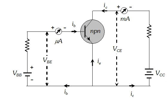 Input characteristic : A graph between the base emitter voltage $V_{B E}$ and the base current at a constant collector emitter voltage $V_{C E}$ is called the input characteristic of the transistor. Output characteristic : A graph between the collector emitter voltage $V_{C E}$ and the collector current $i_{c}$ at a constant base current base current $\dot{l}_{b}$ is called the output characteristic of the transistor
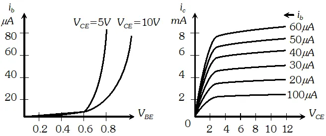
India's Best Exam Preparation for Class 12th - Download Now
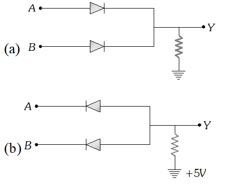
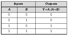
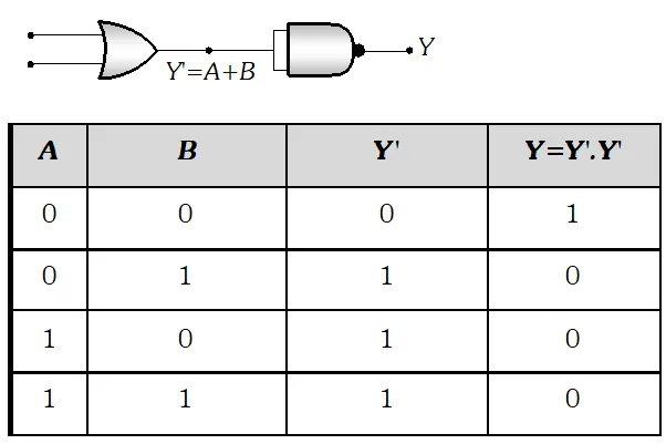
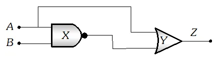
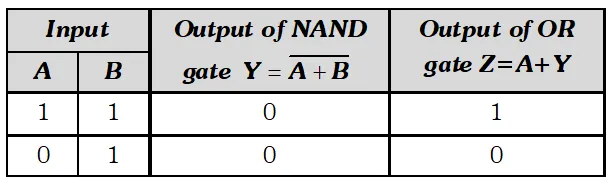
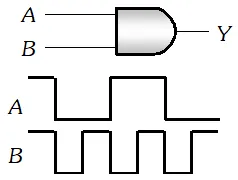
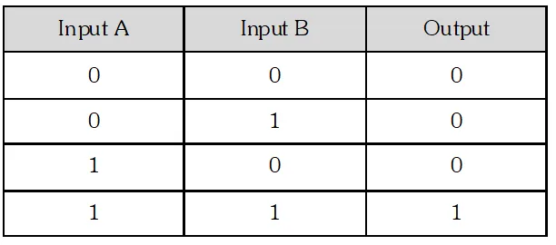
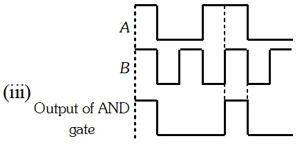
 (b) The given circuit represents AND gate
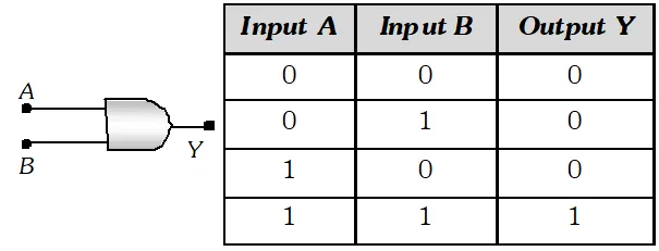
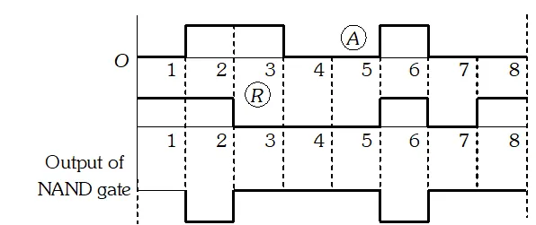
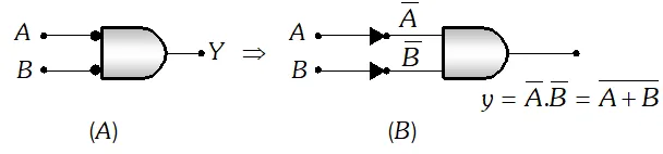 The Boolean expression for output of this gate is $y=\bar{A} \bar{B}=\overline{A+B}$ (From De-Morgan’s theorem) As, $y=\overline{A+B}$ is the Boolean expression for NOR gate, hence bubbled, AND gate acts as NOR gate
 India's Best Exam Preparation for Class 12th - Download Now
Conclusion and Next Steps
Frequently Asked Questions
Comments