Semiconductor Electronics Class 12 Notes - IIT JEE | NEET
Semiconductor Electronics is an important Class 12 Physics chapter for JEE Main, NEET, and Boards covering semiconductors, energy bands, intrinsic and extrinsic semiconductors, p-n junction diodes, rectifiers, transistors, logic gates, and electronic devices with key concepts like doping, forward/reverse bias, current gain, and digital circuits.
.webp)
Table of Contents
- What Are Semiconductors?
- Energy Bands: Conductor vs Semiconductor vs Insulator
- Types of Semiconductors: Intrinsic and Extrinsic
- P-N Junction Diode: How It Works
- Rectifiers: Half Wave and Full Wave
- Transistors: Structure and Applications
- Logic Gates: AND, OR, NOT, NAND, NOR {#logic-gates}
- Key Formulas to Remember for JEE & NEET

eSaral › JEE › NEET ›Semiconductor Electronics Class 12 Notes - IIT JEE | NEET

🚀 Checkout eSaral Courses
What Are Semiconductors?
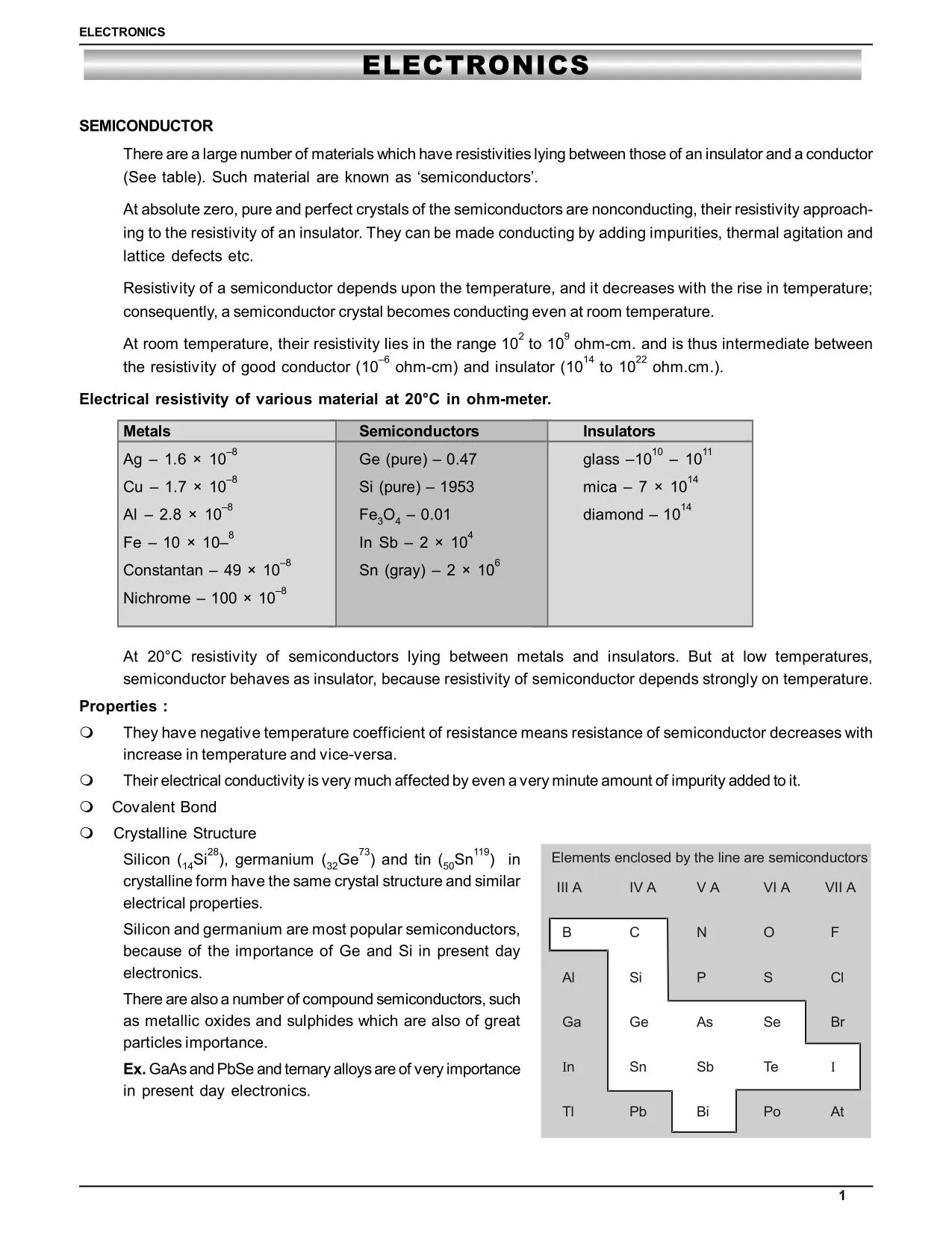
Semiconductors are substances whose electrical conductivity lies between that of conductors and insulators. Unlike conductors, their conductivity increases with temperature — a property that makes them uniquely useful in electronic devices.
Without semiconductors, the electronic devices we use today — smartphones, computers, solar panels, LEDs — would be far too complex and unreliable to manufacture. They are the foundation of modern electronics.
Examples of semiconductors: Silicon (Si), Germanium (Ge)
| Property | Conductor | Semiconductor | Insulator |
|---|---|---|---|
| Conductivity | High (10⁶–10⁸ S/m) | Medium (10⁻⁶–10⁴ S/m) | Very Low (< 10⁻¹¹ S/m) |
| Band gap | Zero or overlap | 0.1–3 eV | > 3 eV |
| Effect of temperature | Conductivity decreases | Conductivity increases | Nearly no change |
| Example | Copper, Silver | Silicon, Germanium | Glass, Rubber |
💡 Expert Tip by Saransh Gupta Sir, IIT Bombay AIR-41: In JEE Main, a very common question asks about the effect of temperature on conductivity. Always remember: in semiconductors, increasing temperature increases conductivity because more electron-hole pairs are generated. In metals, it's the opposite.
India's Best Exam Preparation for Class 12th - Download Now
India's Best Exam Preparation for Class 12th - Download Now
India's Best Exam Preparation for Class 12th - Download Now
eSaral have already come up with an amazing Revision Series of Physics where you can easily revise your chapter within minutes with all the important formulae and key points. This revision series is free for all.
Click Here for Complete Physics Revision Series by Saransh Gupta Sir (AIR-41)
Energy Bands: Conductor vs Semiconductor vs Insulator
What Is an Energy Band?
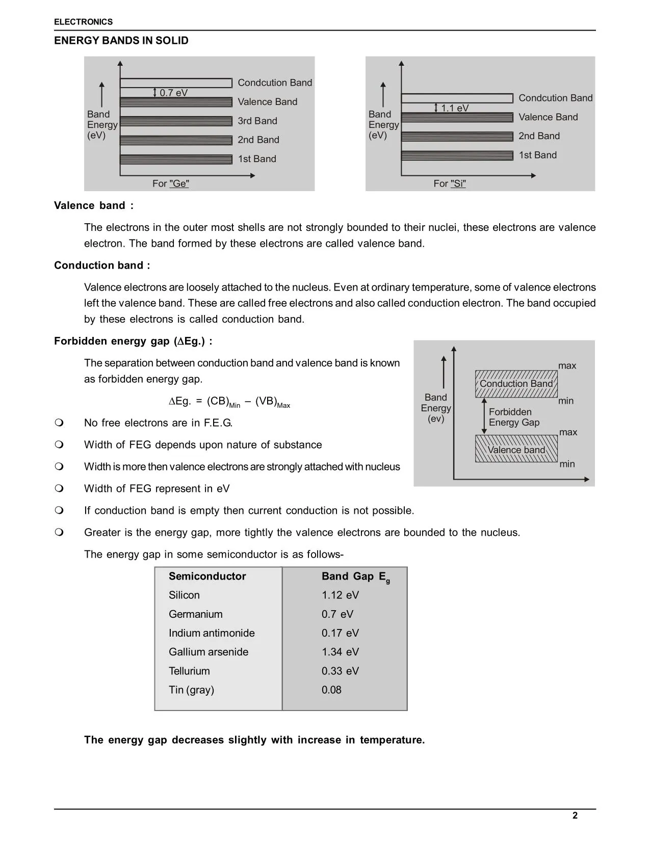
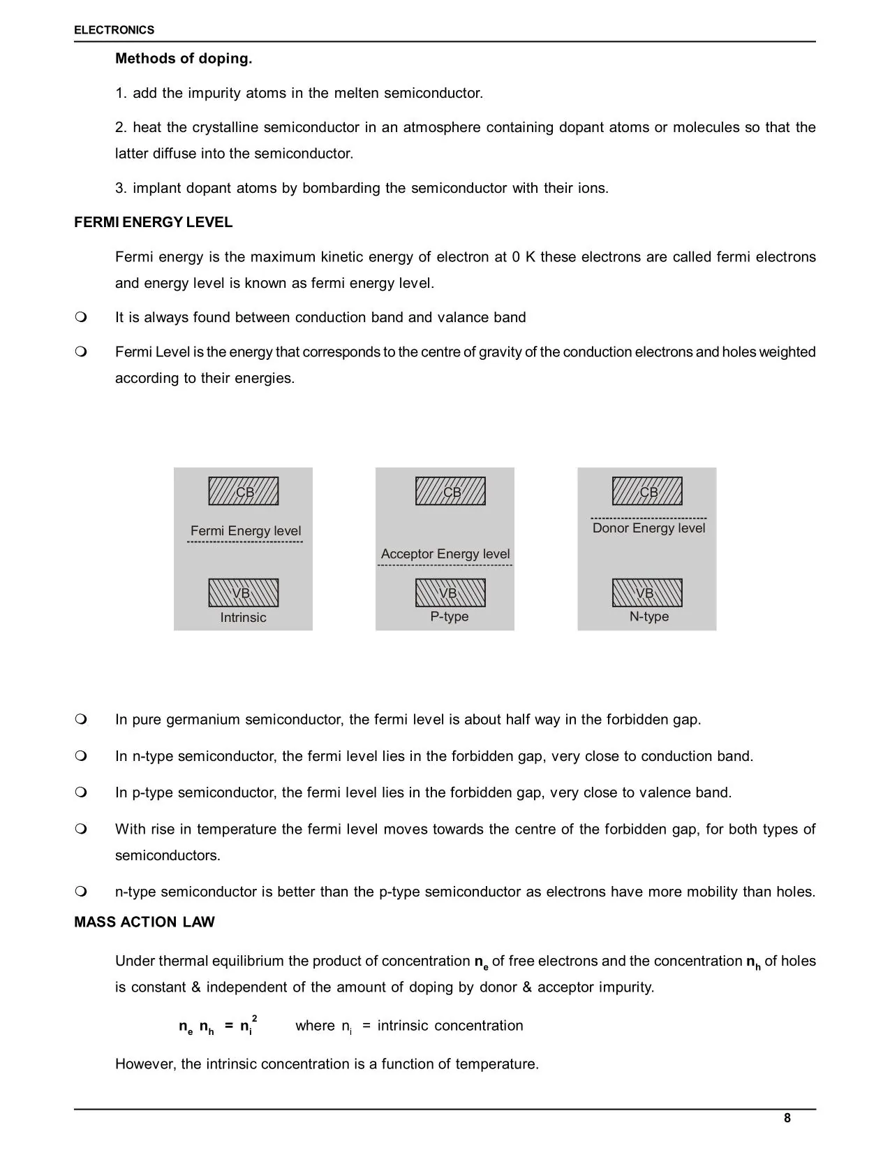
In a single isolated atom, electrons occupy fixed energy levels. When millions of atoms come together to form a solid, these discrete levels spread into energy bands.
The two most important bands are:
- Valence Band: The highest energy band that is completely filled at absolute zero (0 K). Electrons here are bound to atoms.
- Conduction Band: The band above the valence band. Electrons here are free to move and conduct electricity.
- Forbidden Gap (Band Gap): The energy difference between the valence band and conduction band. No electron can exist here.
How Does the Band Gap Determine Material Type?
The size of the forbidden gap determines whether a material is a conductor, semiconductor, or insulator.
- Conductor: Valence and conduction bands overlap. Electrons move freely. Band gap ≈ 0 eV.
- Semiconductor: Small band gap (Si = 1.1 eV, Ge = 0.7 eV). At room temperature, some electrons gain enough energy to jump to the conduction band.
- Insulator: Large band gap (> 3 eV, e.g., diamond = 5.4 eV). Electrons cannot jump to conduction band under normal conditions.
What Is a Hole?
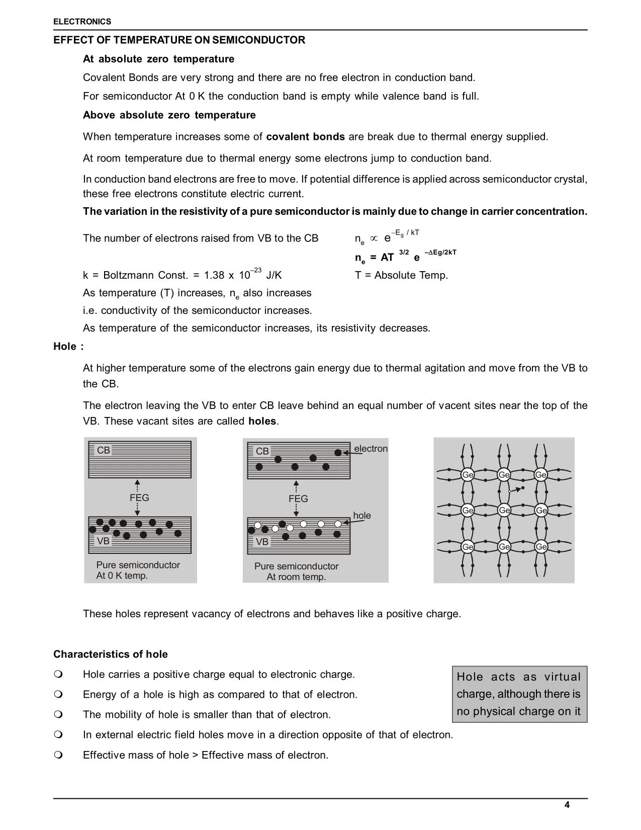
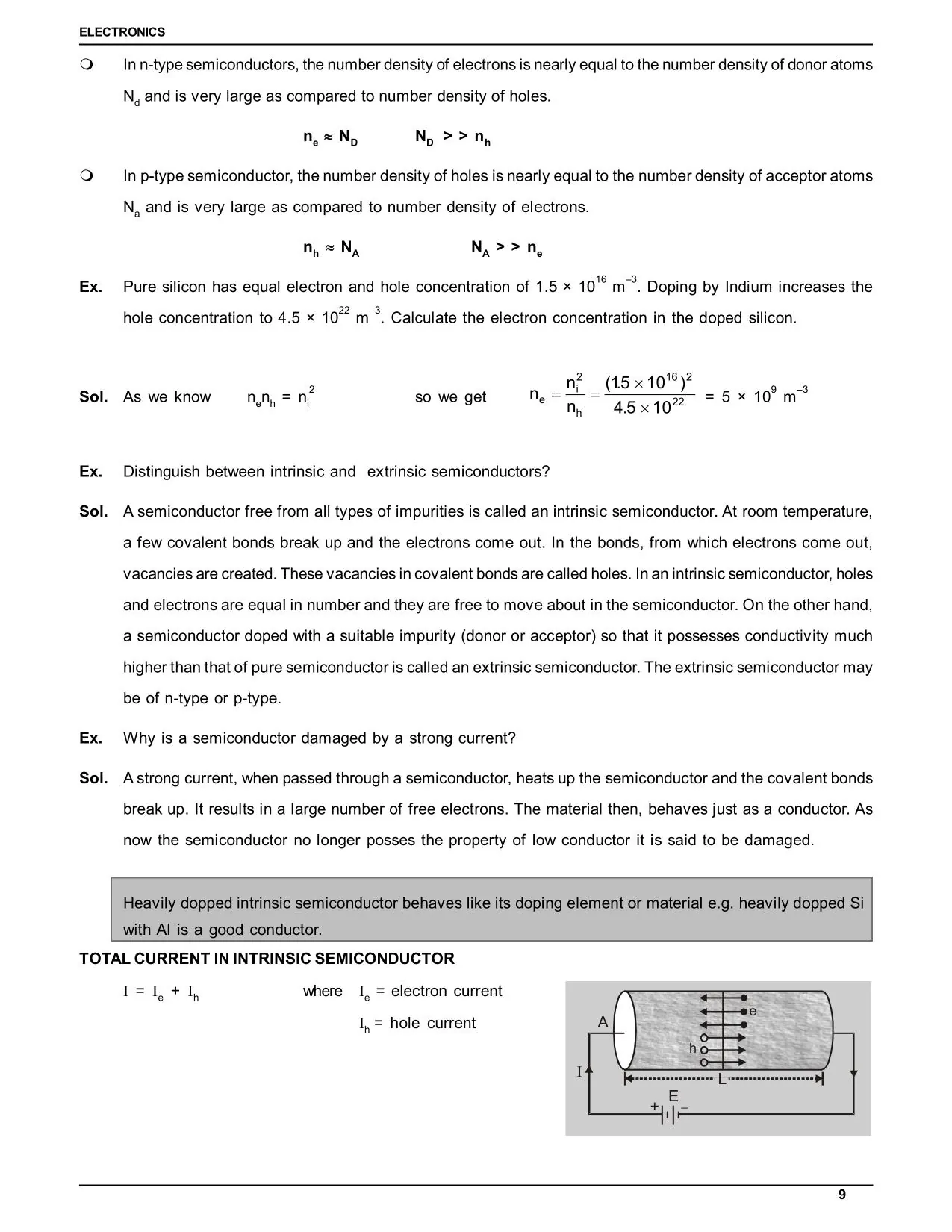
When an electron jumps from the valence band to the conduction band, it leaves behind a vacancy called a hole. A hole behaves like a positive charge carrier. In semiconductors, both electrons (in the conduction band) and holes (in the valence band) contribute to current flow.
Types of Semiconductors: Intrinsic and Extrinsic
What Is an Intrinsic Semiconductor?
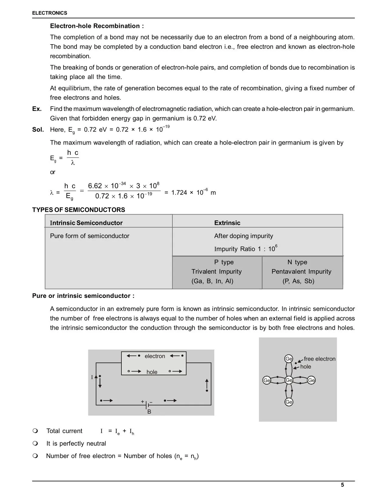
A pure semiconductor with no impurities is called an intrinsic semiconductor. In Silicon, each atom forms 4 covalent bonds. At absolute zero, no free electrons exist. At room temperature, some bonds break, creating electron-hole pairs.
Key relation: n_e = n_h = n_i (number of electrons = number of holes = intrinsic carrier concentration)
What Is an Extrinsic Semiconductor?
When a small amount of impurity is added to an intrinsic semiconductor, it becomes an extrinsic semiconductor. This process is called doping.
There are two types:
N-type Semiconductor
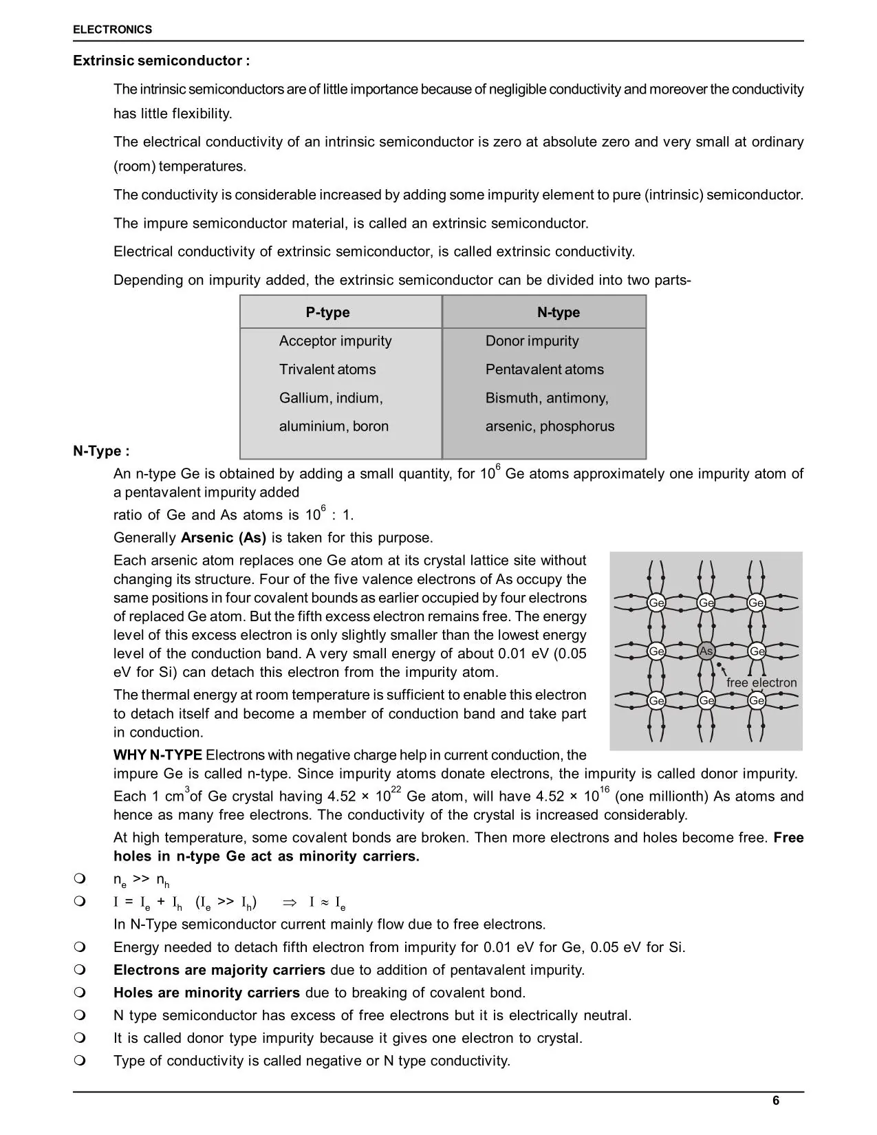
- Doped with pentavalent atoms (5 valence electrons): Phosphorus (P), Arsenic (As), Antimony (Sb)
- The extra (5th) electron becomes a free electron
- Majority carriers: electrons | Minority carriers: holes
- The impurity atom is called a donor atom
P-type Semiconductor
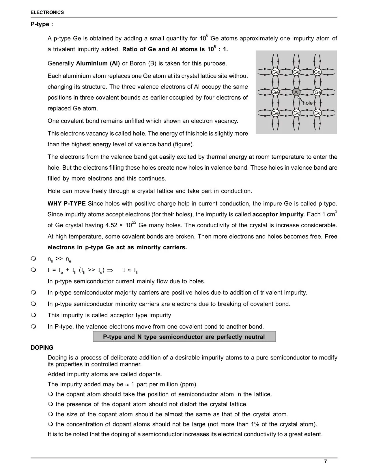
- Doped with trivalent atoms (3 valence electrons): Boron (B), Aluminium (Al), Indium (In)
- The missing bond creates a hole
- Majority carriers: holes | Minority carriers: electrons
- The impurity atom is called an acceptor atom
| Property | N-type | P-type |
|---|---|---|
| Dopant valency | 5 (pentavalent) | 3 (trivalent) |
| Majority carriers | Electrons | Holes |
| Minority carriers | Holes | Electrons |
| Impurity atom | Donor | Acceptor |
| Example dopant | Phosphorus, Arsenic | Boron, Indium |
💡 Expert Tip by Saransh Gupta Sir, IIT Bombay AIR-41: NEET frequently asks: "In an N-type semiconductor, which is the majority carrier?" The answer is electrons. Remember — in N-type, N stands for Negative charge carriers (electrons). Never confuse the overall charge of the semiconductor (which is neutral) with the majority carrier type.
P-N Junction Diode: How It Works
How Is a P-N Junction Formed?
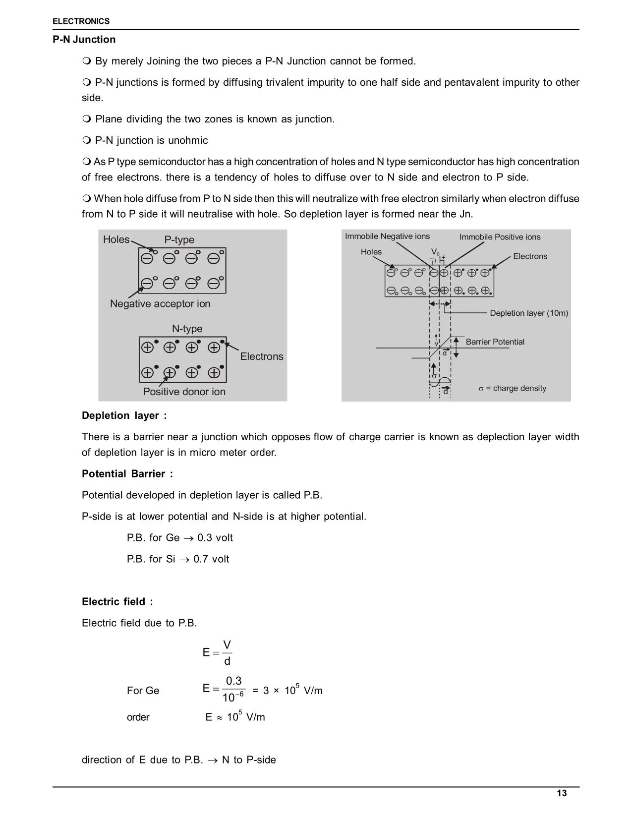
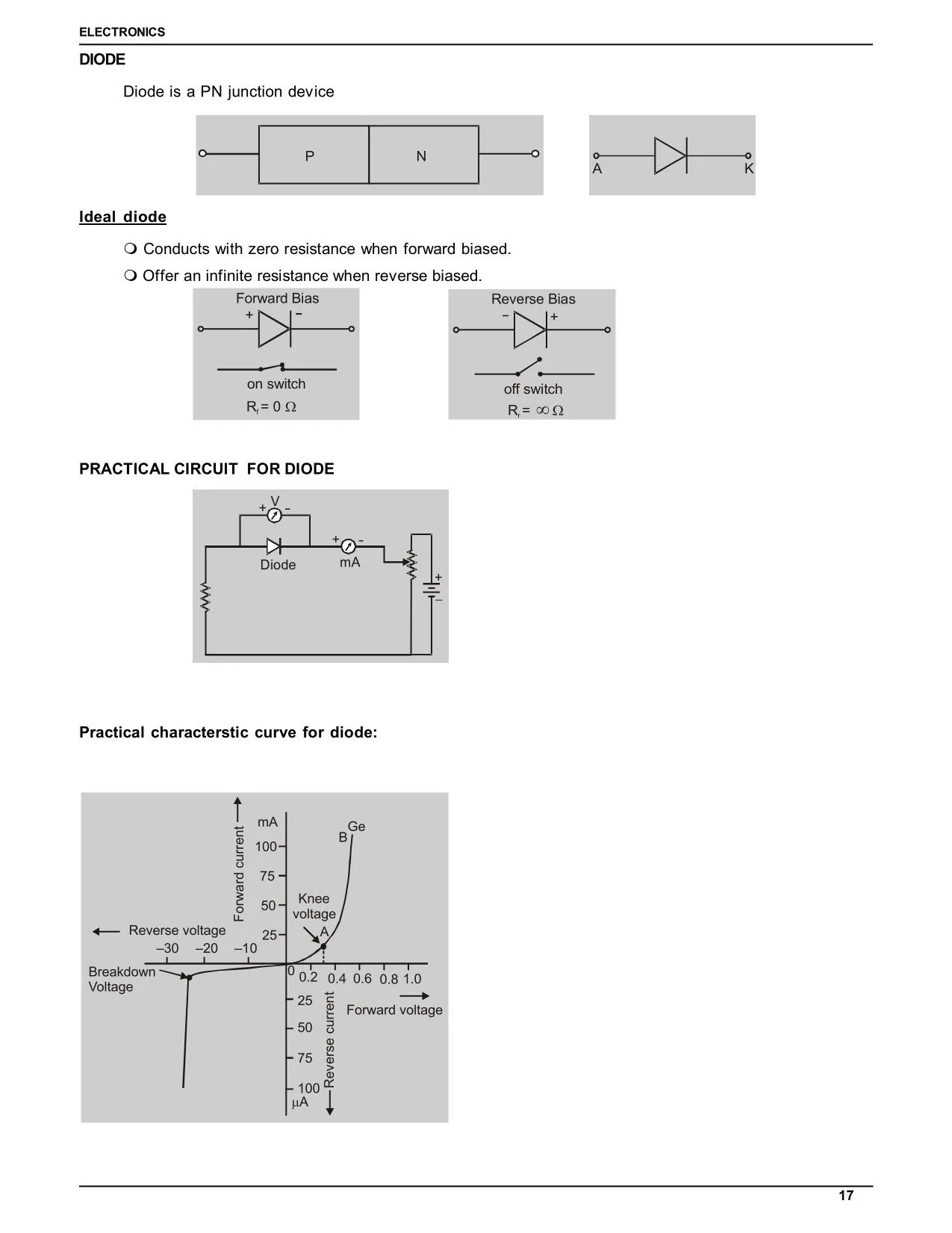
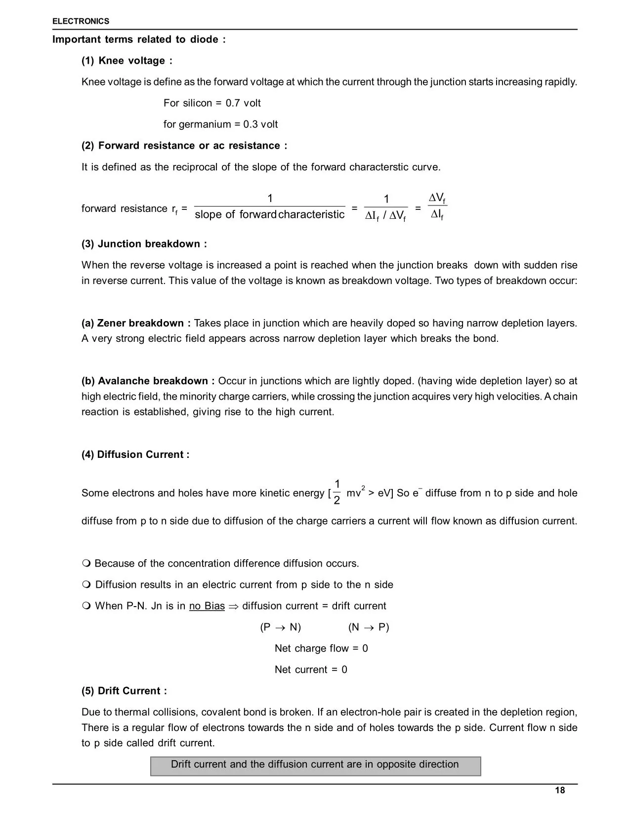
When a P-type and an N-type semiconductor are joined together, a P-N junction is formed. At the junction, electrons from the N-side diffuse to the P-side, and holes from the P-side diffuse to the N-side. This creates a depletion layer — a region depleted of mobile charge carriers — and a built-in electric field called the barrier potential (≈ 0.3 V for Ge, ≈ 0.7 V for Si).
Forward Bias vs Reverse Bias
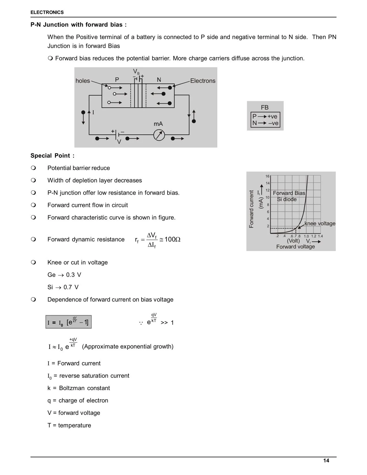
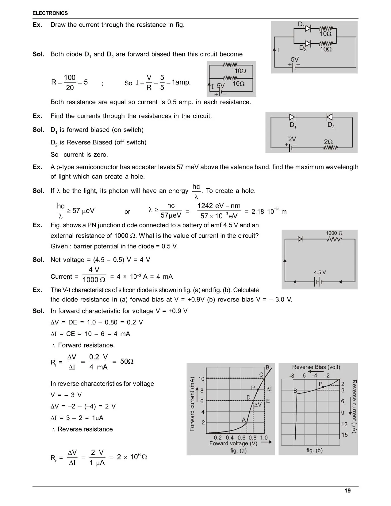
Forward Bias: P-side connected to +ve terminal, N-side to –ve terminal.
- External voltage opposes the barrier potential
- Depletion layer narrows
- Current flows (threshold: ~0.7 V for Si, ~0.3 V for Ge)
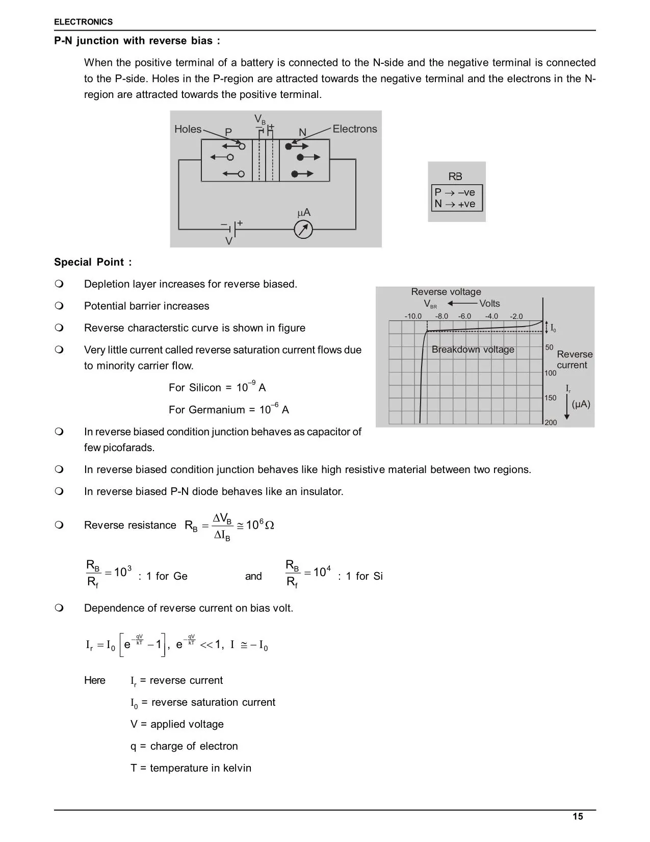
Reverse Bias: P-side connected to –ve terminal, N-side to +ve terminal.
- External voltage adds to the barrier potential
- Depletion layer widens
- Only a tiny reverse saturation current flows (due to minority carriers)
| Parameter | Forward Bias | Reverse Bias |
|---|---|---|
| Depletion layer | Narrows | Widens |
| Resistance | Low | Very high |
| Current | Large (mA range) | Negligible (μA range) |
| Application | Current flow | Blocking |
Special Diodes to Know for JEE & NEET
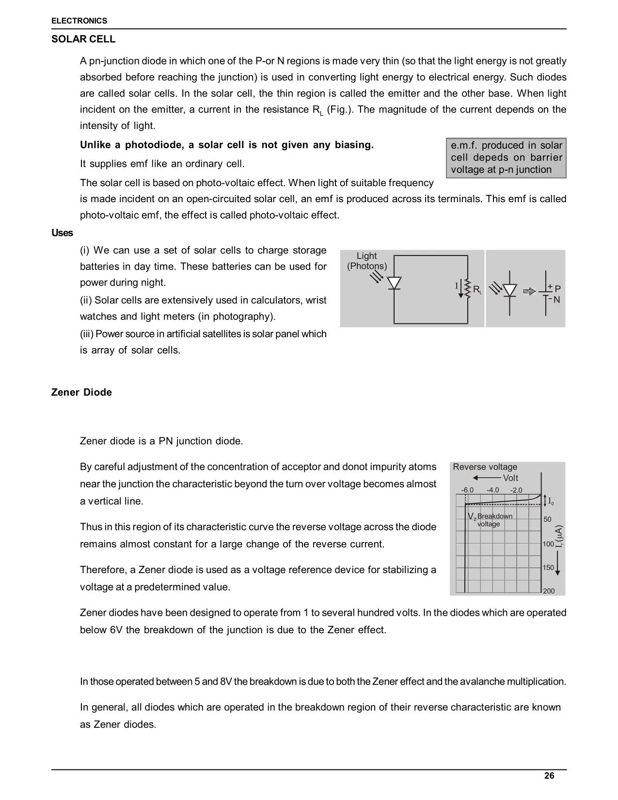
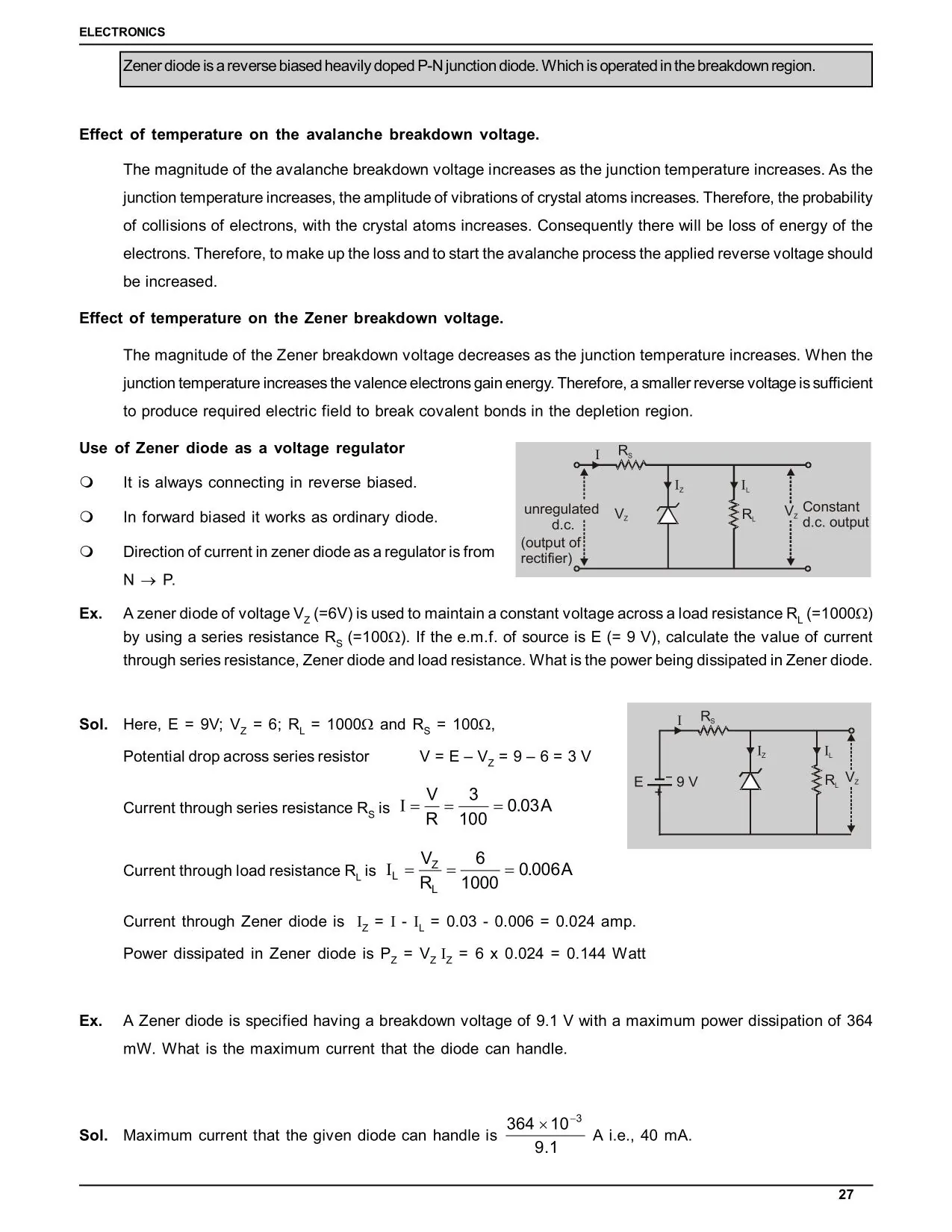
- Zener Diode: Operates in reverse breakdown. Used as a voltage regulator.
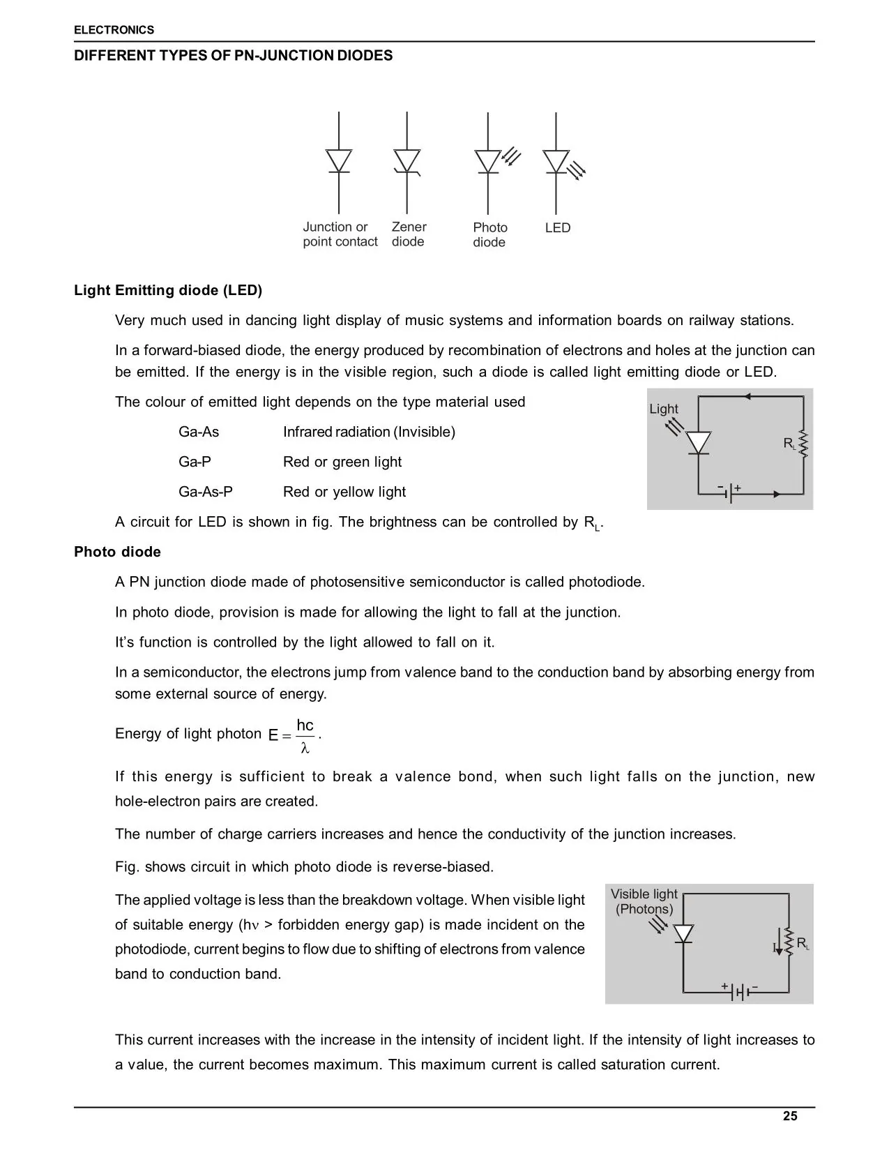
- LED (Light Emitting Diode): Emits light when forward biased. Energy gap determines colour of emitted light.
- Photodiode: Reverse biased; used for detecting light intensity.
- Solar Cell: Converts light energy to electrical energy using the photovoltaic effect.
Rectifiers: Half Wave and Full Wave
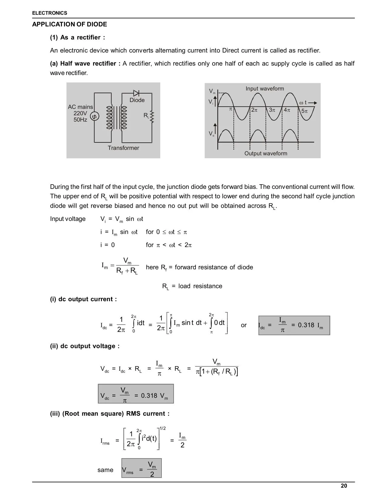
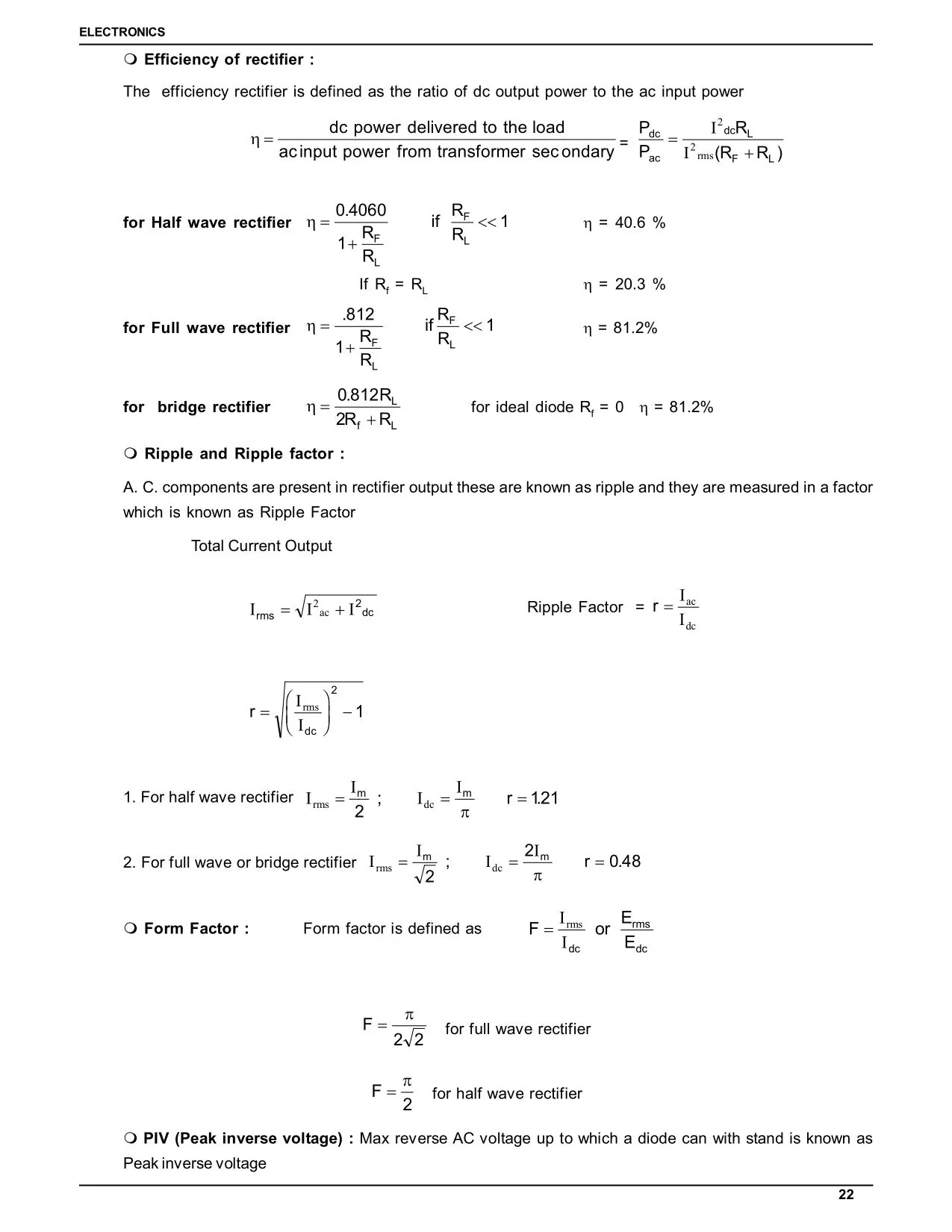
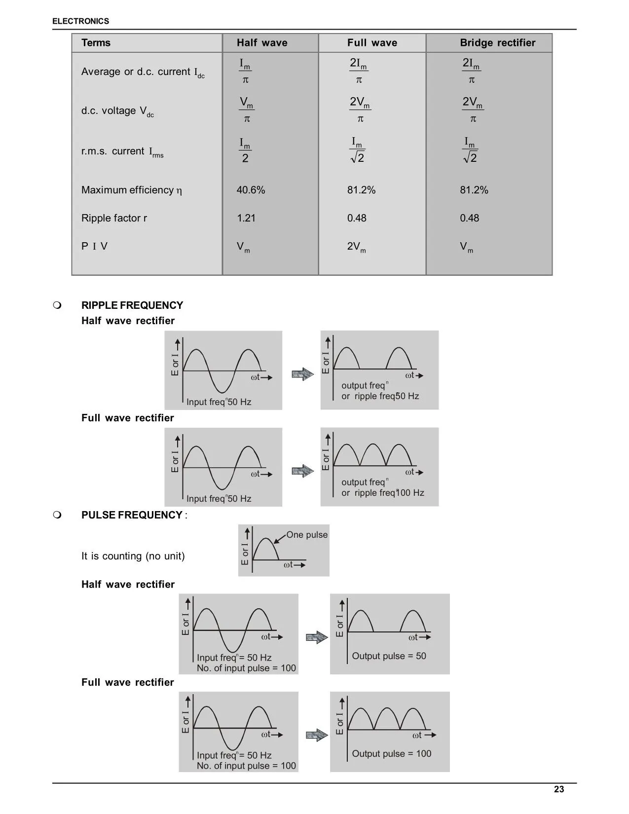
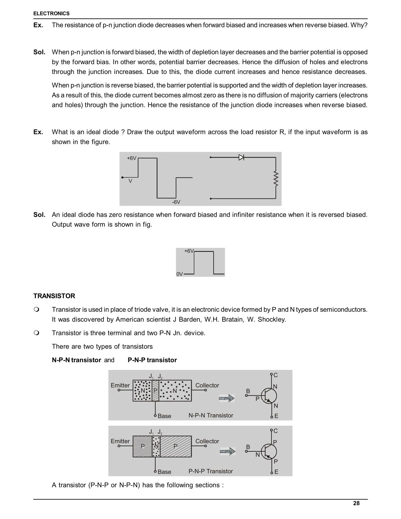
A rectifier converts AC (alternating current) to DC (direct current) using the unidirectional property of a p-n junction diode.
Half Wave Rectifier
- Uses 1 diode
- Only the positive half cycle of AC passes through
- Output is pulsating DC
- Efficiency: ~40.6%
- Output frequency = Input frequency
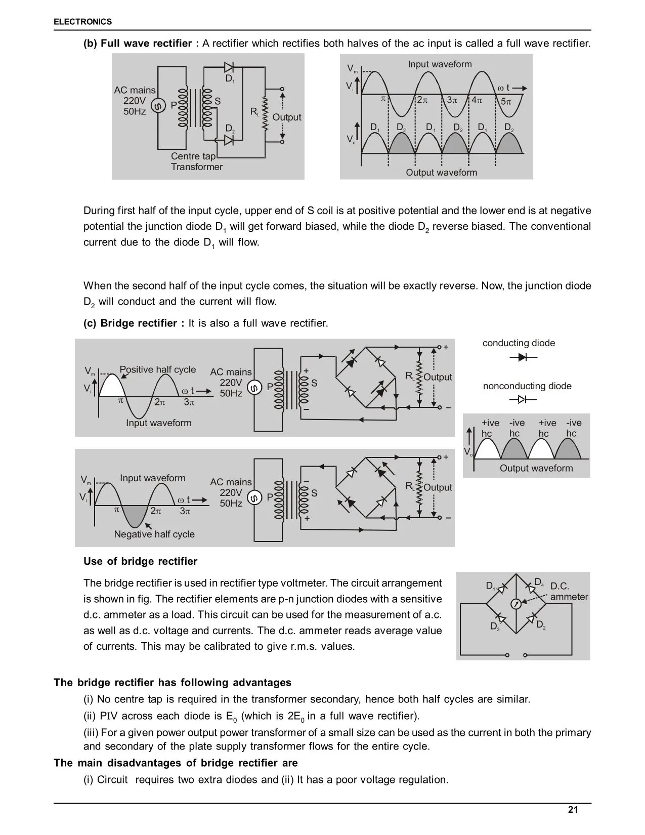
Full Wave Rectifier
- Uses 2 diodes (centre-tap) or 4 diodes (bridge rectifier)
- Both halves of AC are utilised
- Efficiency: ~81.2% — nearly double that of half wave
- Output frequency = 2 × Input frequency
| Type | Diodes Used | Efficiency | Output Frequency |
|---|---|---|---|
| Half Wave | 1 | ~40.6% | f |
| Full Wave (Centre Tap) | 2 | ~81.2% | 2f |
| Full Wave (Bridge) | 4 | ~81.2% | 2f |
Transistors: Structure and Applications
What Is a Transistor?
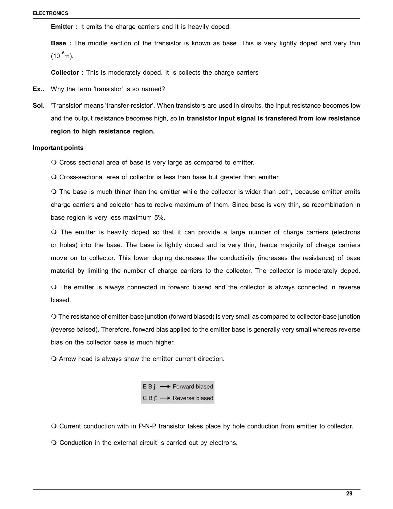
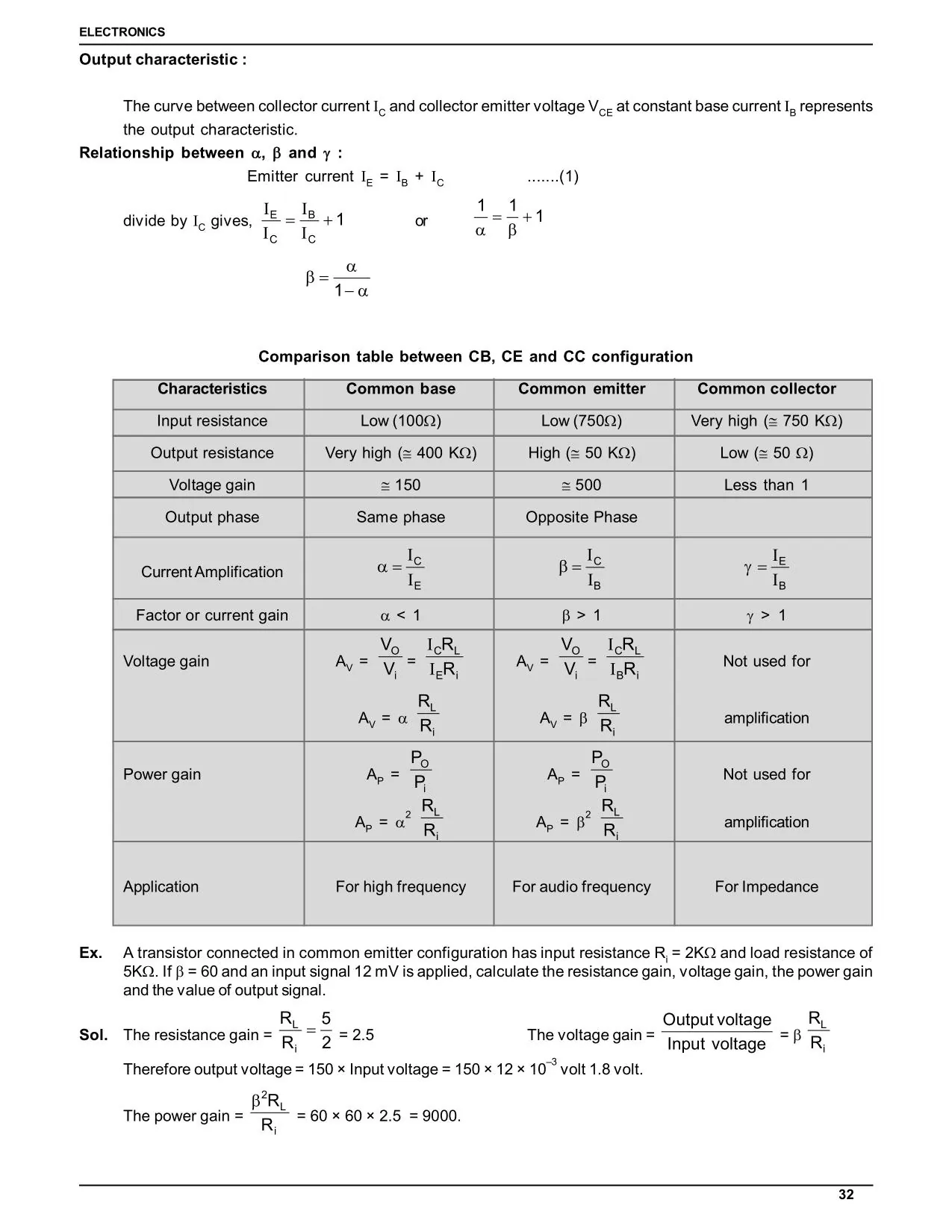
A transistor is a three-layer semiconductor device used for amplification and switching. It has three terminals: Emitter (E), Base (B), and Collector (C).
There are two types:
- NPN transistor: Two N-type layers sandwiching a thin P-type layer
- PNP transistor: Two P-type layers sandwiching a thin N-type layer
The base region is always very thin and lightly doped. The emitter is heavily doped. The collector has the largest area.
Transistor Configurations
Three configurations are used:
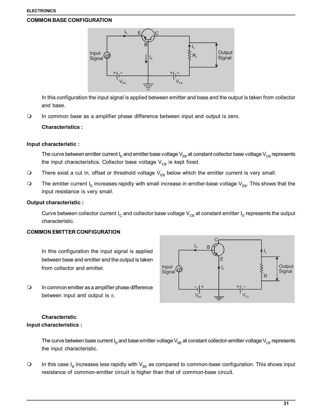
- Common Base (CB): Input at emitter, output at collector. Current gain (α) < 1.
- Common Emitter (CE): Input at base, output at collector. Current gain (β) >> 1. Most widely used.
- Common Collector (CC): Input at base, output at emitter. Used as a buffer.
Key Transistor Relations
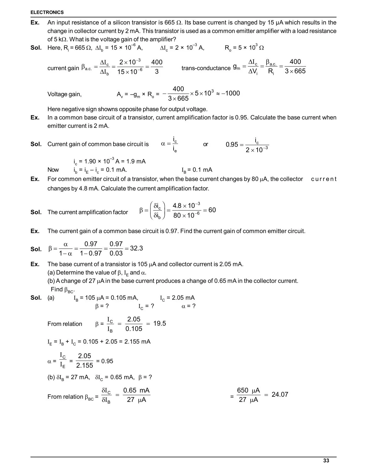
- α = I_C / I_E (common base current gain; always < 1)
- β = I_C / I_B (common emitter current gain; typically 20–500)
- β = α / (1 – α)
- I_E = I_B + I_C
Transistor as a Switch
In saturation mode (both junctions forward biased) → transistor is ON (acts like closed switch). In cut-off mode (both junctions reverse biased) → transistor is OFF (acts like open switch).
Logic Gates: AND, OR, NOT, NAND, NOR {#logic-gates}
Logic gates are the building blocks of digital circuits. They perform Boolean operations on binary inputs (0 and 1).
| Gate | Symbol | Operation | Output is 1 when… |
|---|---|---|---|
| AND | A · B | Multiplication | Both inputs are 1 |
| OR | A + B | Addition | At least one input is 1 |
| NOT | Ā | Inversion | Input is 0 |
| NAND | NOT of AND | ¬(A·B) | Not both inputs are 1 |
| NOR | NOT of OR | ¬(A+B) | Both inputs are 0 |
| XOR | A ⊕ B | Exclusive OR | Inputs are different |
Truth Tables (AND, OR, NOT)
AND Gate:
| A | B | Output |
|---|---|---|
| 0 | 0 | 0 |
| 0 | 1 | 0 |
| 1 | 0 | 0 |
| 1 | 1 | 1 |
OR Gate:
| A | B | Output |
|---|---|---|
| 0 | 0 | 0 |
| 0 | 1 | 1 |
| 1 | 0 | 1 |
| 1 | 1 | 1 |
NOT Gate:
| A | Output |
|---|---|
| 0 | 1 |
| 1 | 0 |
NAND and NOR gates are called Universal Gates because any other logic gate can be constructed using only NAND gates or only NOR gates. This is a guaranteed JEE Main question at least once every 2–3 years.
Key Formulas to Remember for JEE & NEET
| Formula | Description |
|---|---|
| n_e × n_h = n_i² | Mass action law (applies to both intrinsic and extrinsic semiconductors) |
| I_E = I_B + I_C | Transistor current relation |
| α = I_C / I_E | Common base current gain |
| β = I_C / I_B | Common emitter current gain |
| β = α / (1 – α) | Relation between α and β |
| V_barrier (Si) ≈ 0.7 V | Potential barrier for Silicon p-n junction |
| V_barrier (Ge) ≈ 0.3 V | Potential barrier for Germanium p-n junction |
| Output frequency (full wave) = 2f | Full wave rectifier output frequency |
| E = hν | Energy of photon emitted by LED |
Frequently Asked Questions
Find answers to common questions.
What is the difference between a conductor, semiconductor, and insulator in Class 12?
The key difference lies in the band gap. Conductors have zero or overlapping band gaps, so electrons flow freely. Semiconductors have a small band gap (0.1–3 eV) — some electrons can cross it at room temperature. Insulators have a large band gap (> 3 eV), so no electron crosses it under normal conditions.
What are the two types of semiconductors in Class 12 Physics?
The two types are intrinsic (pure) and extrinsic (doped) semiconductors. Intrinsic semiconductors are pure Silicon or Germanium. Extrinsic semiconductors are doped with impurities — pentavalent dopants create N-type (majority carriers: electrons), while trivalent dopants create P-type (majority carriers: holes).
What is a p-n junction and why does a depletion layer form?
p-n junction is formed when P-type and N-type semiconductors are joined. At the junction, electrons from N-side and holes from P-side diffuse across and recombine, creating a depletion layer — a region free of mobile charges. This region creates a built-in electric field (barrier potential) that opposes further diffusion.
What is the difference between forward bias and reverse bias of a diode?
In forward bias, the positive terminal connects to P-side and negative to N-side. This reduces the barrier, and current flows above the threshold voltage (~0.7 V for Si). In reverse bias, connections are reversed — the barrier increases, the depletion layer widens, and current flow is negligible except for tiny minority carrier current.
How many questions come from Semiconductor Electronics in JEE Main?
Semiconductor Electronics typically contributes 1–2 questions in JEE Main, worth 4–8 marks. High-frequency topics are p-n junction biasing, transistor current gain (α and β), logic gates truth tables, and Zener diode applications. In NEET, 1 question from this chapter appears almost every year, usually from p-n junction or transistor basics.